PIC18LF47J53-I/ML Microchip Technology, PIC18LF47J53-I/ML Datasheet - Page 311
PIC18LF47J53-I/ML
Manufacturer Part Number
PIC18LF47J53-I/ML
Description
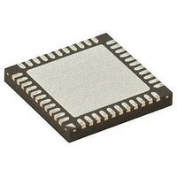
IC PIC MCU 128KB FLASH 44QFN
Manufacturer
Microchip Technology
Series
PIC® XLP™ 18Fr
Datasheets
1.PIC18LF24J10-ISS.pdf
(32 pages)
2.PIC18F26J13-ISS.pdf
(496 pages)
3.PIC18F26J53-ISS.pdf
(586 pages)
4.PIC18F26J53-ISS.pdf
(12 pages)
Specifications of PIC18LF47J53-I/ML
Core Size
8-Bit
Program Memory Size
128KB (64K x 16)
Core Processor
PIC
Speed
48MHz
Connectivity
I²C, LIN, SPI, UART/USART, USB
Peripherals
Brown-out Detect/Reset, POR, PWM, WDT
Number Of I /o
34
Program Memory Type
FLASH
Ram Size
3.8K x 8
Voltage - Supply (vcc/vdd)
2 V ~ 2.75 V
Data Converters
A/D 13x10b/12b
Oscillator Type
Internal
Operating Temperature
-40°C ~ 85°C
Package / Case
*
Controller Family/series
PIC18
Cpu Speed
48MHz
Digital Ic Case Style
QFN
Supply Voltage Range
1.8V To 3.6V
Embedded Interface Type
I2C, SPI, USART
Rohs Compliant
Yes
Lead Free Status / RoHS Status
Lead free / RoHS Compliant
Eeprom Size
-
Lead Free Status / RoHS Status
Lead free / RoHS Compliant, Lead free / RoHS Compliant


REGISTER 20-5:
2010 Microchip Technology Inc.
bit 7
Legend:
R = Readable bit
-n = Value at POR
bit 7
bit 6
bit 5
bit 4
bit 3
bit 2
bit 1
bit 0
Note 1:
R/W-1
SMP
2:
3:
This bit is cleared on Reset and when SSPEN is cleared.
This bit holds the R/W bit information following the last address match. This bit is only valid from the
address match to the next Start bit, Stop bit or not ACK bit.
ORing this bit with SEN, RSEN, PEN, RCEN or ACKEN will indicate if the MSSPx is in Active mode.
SMP: Slew Rate Control bit
In Master or Slave mode:
1 = Slew rate control disabled for Standard Speed mode (100 kHz and 1 MHz)
0 = Slew rate control enabled for High-Speed mode (400 kHz)
CKE: SMBus Select bit
In Master or Slave mode:
1 = Enable SMBus specific inputs
0 = Disable SMBus specific inputs
D/A: Data/Address bit
In Master mode:
Reserved.
In Slave mode:
1 = Indicates that the last byte received or transmitted was data
0 = Indicates that the last byte received or transmitted was address
P: Stop bit
1 = Indicates that a Stop bit has been detected last
0 = Stop bit was not detected last
S: Start bit
1 = Indicates that a Start bit has been detected last
0 = Start bit was not detected last
R/W: Read/Write Information bit
In Slave mode:
1 = Read
0 = Write
In Master mode:
1 = Transmit is in progress
0 = Transmit is not in progress
UA: Update Address bit (10-Bit Slave mode only)
1 = Indicates that the user needs to update the address in the SSPxADD register
0 = Address does not need to be updated
BF: Buffer Full Status bit
In Transmit mode:
1 = SSPxBUF is full
0 = SSPxBUF is empty
In Receive mode:
1 = SSPxBUF is full (does not include the ACK and Stop bits)
0 = SSPxBUF is empty (does not include the ACK and Stop bits)
R/W-1
CKE
SSPxSTAT: MSSPx STATUS REGISTER (I
(1)
(1)
W = Writable bit
‘1’ = Bit is set
D/A
R-1
(2,3)
R-1
P
Preliminary
(1)
U = Unimplemented bit, read as ‘0’
‘0’ = Bit is cleared
PIC18F47J53 FAMILY
R-1
S
(1)
2
C™ MODE) (1, ACCESS FC7h; 2, F73h)
R/W
R-1
(2,3)
x = Bit is unknown
R-1
UA
DS39964B-page 311
R-1
BF
bit 0
Related parts for PIC18LF47J53-I/ML
Image
Part Number
Description
Manufacturer
Datasheet
Request
R

Part Number:
Description:
Manufacturer:
Microchip Technology Inc.
Datasheet:
Part Number:
Description:
Manufacturer:
Microchip Technology Inc.
Datasheet:
Part Number:
Description:
Manufacturer:
Microchip Technology Inc.
Datasheet:
Part Number:
Description:
Manufacturer:
Microchip Technology Inc.
Datasheet:
Part Number:
Description:
Manufacturer:
Microchip Technology Inc.
Datasheet:
Part Number:
Description:
Manufacturer:
Microchip Technology Inc.
Datasheet:
Part Number:
Description:
Manufacturer:
Microchip Technology Inc.
Datasheet:
Part Number:
Description:
Manufacturer:
Microchip Technology Inc.
Datasheet: