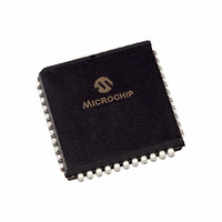
PIC16C662-04/L Microchip Technology, PIC16C662-04/L Datasheet - Page 15

PIC16C662-04/L
Manufacturer Part Number
PIC16C662-04/L
Description
IC MCU OTP 4KX14 COMP 44PLCC
Manufacturer
Microchip Technology
Series
PIC® 16Cr
Specifications of PIC16C662-04/L
Core Size
8-Bit
Program Memory Size
7KB (4K x 14)
Core Processor
PIC
Speed
4MHz
Peripherals
Brown-out Detect/Reset, LED, POR, WDT
Number Of I /o
33
Program Memory Type
OTP
Ram Size
176 x 8
Voltage - Supply (vcc/vdd)
4 V ~ 6 V
Oscillator Type
External
Operating Temperature
0°C ~ 70°C
Package / Case
44-PLCC
Controller Family/series
PIC16C
No. Of I/o's
33
Ram Memory Size
176Byte
Cpu Speed
4MHz
No. Of Timers
1
Processor Series
PIC16C
Core
PIC
Data Bus Width
8 bit
Data Ram Size
176 B
Interface Type
RS- 232
Maximum Clock Frequency
4 MHz
Number Of Programmable I/os
33
Number Of Timers
8
Operating Supply Voltage
3 V to 6 V
Maximum Operating Temperature
+ 70 C
Mounting Style
SMD/SMT
3rd Party Development Tools
52715-96, 52716-328, 52717-734
Development Tools By Supplier
ICE2000, DM163022
Minimum Operating Temperature
0 C
On-chip Adc
10 bit
Data Rom Size
176 B
Height
3.87 mm
Length
16.59 mm
Supply Voltage (max)
6 V
Supply Voltage (min)
4 V
Width
16.59 mm
Lead Free Status / RoHS Status
Lead free / RoHS Compliant
For Use With
DVA16XL441 - ADAPTER DEVICE ICE 44PLCC309-1040 - ADAPTER 44-PLCC ZIF TO 40-DIP309-1039 - ADAPTER 44-PLCC TO 40-DIP
Eeprom Size
-
Data Converters
-
Connectivity
-
Lead Free Status / Rohs Status
Details
Available stocks
Company
Part Number
Manufacturer
Quantity
Price
Company:
Part Number:
PIC16C662-04/L
Manufacturer:
Microchip Technology
Quantity:
10 000
3.1
The clock input (from OSC1) is internally divided by
four to generate four non-overlapping quadrature
clocks namely Q1, Q2, Q3, and Q4. Internally, the
program counter (PC) is incremented every Q1, the
instruction is fetched from the program memory and
latched into the instruction register in Q4. The
instruction is decoded and executed during the
following Q1 through Q4. The clocks and instruction
execution flow is shown in Figure 3-3.
FIGURE 3-3:
EXAMPLE 3-1:
1. MOVLW 55h
2. MOVWF PORTB
3. CALL SUB_1
4. BSF
5. Instruction @ address SUB_1
1996 Microchip Technology Inc.
All instructions are single cycle, except for any program branches. These take two cycles since the fetch
instruction is “flushed” from the pipeline while the new instruction is being fetched and then executed.
OSC2/CLKOUT
Clocking Scheme/Instruction Cycle
(RC mode)
PORTA, BIT3 (Forced NOP)
OSC1
CLOCK/INSTRUCTION CYCLE
Q4
PC
Q2
Q3
Q1
INSTRUCTION PIPELINE FLOW
Q1
Execute INST (PC-1)
Fetch INST (PC)
Fetch 1
Q2
Tcy0
PC
Q3
Execute 1
Fetch 2
Q4
Tcy1
Preliminary
PIC16C64X & PIC16C66X
Q1
Execute INST (PC)
Execute 2
Fetch INST (PC+1)
Fetch 3
Q2
Tcy2
PC+1
3.2
An “Instruction Cycle” consists of four Q cycles (Q1,
Q2, Q3, and Q4). The instruction fetch and execute are
pipelined such that fetch takes one instruction cycle
while decode and execute takes another instruction
cycle. However, due to the pipelining, each instruction
effectively executes in one cycle. If an instruction
causes the program counter to change (e.g., GOTO )
then two cycles are required to complete the instruction
(Example 3-1).
A fetch cycle begins with the program counter (PC)
incrementing in Q1.
In the execution cycle, the fetched instruction is latched
into the “Instruction Register (IR)” in cycle Q1. This
instruction is then decoded and executed during the
Q2, Q3, and Q4 cycles. Data memory is read during Q2
(operand read) and written during Q4 (destination
write).
Q3
Execute 3
Fetch 4
Instruction Flow/Pipelining
Q4
Tcy3
Q1
Fetch SUB_1 Execute SUB_1
Execute INST (PC+1)
Fetch INST (PC+2)
Q2
Flush
Tcy4
PC+2
Q3
DS30559A-page 15
Q4
Tcy5
Internal
phase
clock


