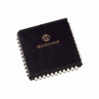
PIC16C662-04/L Microchip Technology, PIC16C662-04/L Datasheet - Page 18

PIC16C662-04/L
Manufacturer Part Number
PIC16C662-04/L
Description
IC MCU OTP 4KX14 COMP 44PLCC
Manufacturer
Microchip Technology
Series
PIC® 16Cr
Specifications of PIC16C662-04/L
Core Size
8-Bit
Program Memory Size
7KB (4K x 14)
Core Processor
PIC
Speed
4MHz
Peripherals
Brown-out Detect/Reset, LED, POR, WDT
Number Of I /o
33
Program Memory Type
OTP
Ram Size
176 x 8
Voltage - Supply (vcc/vdd)
4 V ~ 6 V
Oscillator Type
External
Operating Temperature
0°C ~ 70°C
Package / Case
44-PLCC
Controller Family/series
PIC16C
No. Of I/o's
33
Ram Memory Size
176Byte
Cpu Speed
4MHz
No. Of Timers
1
Processor Series
PIC16C
Core
PIC
Data Bus Width
8 bit
Data Ram Size
176 B
Interface Type
RS- 232
Maximum Clock Frequency
4 MHz
Number Of Programmable I/os
33
Number Of Timers
8
Operating Supply Voltage
3 V to 6 V
Maximum Operating Temperature
+ 70 C
Mounting Style
SMD/SMT
3rd Party Development Tools
52715-96, 52716-328, 52717-734
Development Tools By Supplier
ICE2000, DM163022
Minimum Operating Temperature
0 C
On-chip Adc
10 bit
Data Rom Size
176 B
Height
3.87 mm
Length
16.59 mm
Supply Voltage (max)
6 V
Supply Voltage (min)
4 V
Width
16.59 mm
Lead Free Status / RoHS Status
Lead free / RoHS Compliant
For Use With
DVA16XL441 - ADAPTER DEVICE ICE 44PLCC309-1040 - ADAPTER 44-PLCC ZIF TO 40-DIP309-1039 - ADAPTER 44-PLCC TO 40-DIP
Eeprom Size
-
Data Converters
-
Connectivity
-
Lead Free Status / Rohs Status
Details
Available stocks
Company
Part Number
Manufacturer
Quantity
Price
Company:
Part Number:
PIC16C662-04/L
Manufacturer:
Microchip Technology
Quantity:
10 000
PIC16C64X & PIC16C66X
4.2
The data memory (Figure 4-4) is partitioned into two
banks which contain the general purpose registers and
the special function registers. Bank 0 is selected when
bit RP0 (STATUS<5>) is cleared. Bank 1 is selected
when the RP0 bit is set. The Special Function Regis-
ters are located in the first 32 locations of each Bank.
Register locations A0h-EFh (Bank 1) are general pur-
pose registers implemented as static RAM. Some spe-
cial function registers are mapped in Bank 1.
4.2.1
The register file is organized as 176 x 8 for the
PIC16C642/662, and 128 x8 for the PIC16C641/661.
Each is accessed either directly, or indirectly through
the File Select Register FSR (Section 4.5).
DS30559A-page 18
Data Memory Organization
GENERAL PURPOSE REGISTER FILE
Preliminary
FIGURE 4-3:
Note 1: Not a physical register.
Address
Unimplemented data memory locations, read as '0'.
File
0Ch
0Dh
1Ch
1Dh
0Ah
0Bh
0Eh
1Ah
1Bh
1Eh
0Fh
1Fh
7Fh
00h
01h
02h
03h
04h
05h
06h
07h
08h
09h
10h
12h
13h
14h
15h
16h
17h
18h
19h
20h
11h
2: Not implemented on the PIC16C641.
PORTD
PORTE
STATUS
PCLATH
INTCON
CMCON
PORTC
INDF
PORTA
PORTB
Bank 0
Purpose
Register
TMR0
General
PIR1
FSR
PCL
PIC16C641/661 DATA
MEMORY MAP
(1)
(2)
(2)
1996 Microchip Technology Inc.
in Page 0
Purpose
Register
General
Mapped
OPTION
STATUS
TRISD
TRISE
PCLATH
INTCON
VRCON
INDF
Bank 1
TRISA
TRISB
TRISC
PCON
PIE1
FSR
PCL
(1)
(2)
(2)
Address
80h
81h
82h
83h
84h
85h
86h
87h
88h
89h
8Ah
8Bh
8Ch
8Dh
8Eh
8Fh
90h
91h
92h
93h
94h
95h
96h
97h
98h
99h
9Ah
9Bh
9Ch
9Dh
9Eh
9Fh
A0h
BFh
C0h
EFh
FFh
F0h
File


