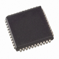
AT89C51RC2-SLSUM Atmel, AT89C51RC2-SLSUM Datasheet - Page 18

AT89C51RC2-SLSUM
Manufacturer Part Number
AT89C51RC2-SLSUM
Description
IC 8051 MCU FLASH 32K 44PLCC
Manufacturer
Atmel
Series
89Cr
Datasheet
1.AT89C51RB2-RLTIL.pdf
(127 pages)
Specifications of AT89C51RC2-SLSUM
Core Processor
8051
Core Size
8-Bit
Speed
60MHz
Connectivity
SPI, UART/USART
Peripherals
POR, PWM, WDT
Number Of I /o
32
Program Memory Size
32KB (32K x 8)
Program Memory Type
FLASH
Ram Size
1.25K x 8
Voltage - Supply (vcc/vdd)
2.7 V ~ 5.5 V
Oscillator Type
External
Operating Temperature
-40°C ~ 85°C
Package / Case
44-PLCC
Cpu Family
89C
Device Core
8051
Device Core Size
8b
Frequency (max)
60MHz
Interface Type
SPI/UART
Total Internal Ram Size
1.25KB
# I/os (max)
32
Number Of Timers - General Purpose
3
Operating Supply Voltage (typ)
3.3/5V
Operating Supply Voltage (max)
5.5V
Operating Supply Voltage (min)
2.7V
Instruction Set Architecture
CISC
Operating Temp Range
-40C to 85C
Operating Temperature Classification
Industrial
Mounting
Surface Mount
Pin Count
44
Package Type
PLCC
Processor Series
AT89x
Core
8051
Data Bus Width
8 bit
Data Ram Size
1280 B
Maximum Clock Frequency
60 MHz
Number Of Programmable I/os
32
Number Of Timers
3
Operating Supply Voltage
2.7 V to 5.5 V
Maximum Operating Temperature
+ 85 C
Mounting Style
SMD/SMT
3rd Party Development Tools
PK51, CA51, A51, ULINK2
Minimum Operating Temperature
- 40 C
For Use With
AT89STK-11 - KIT STARTER FOR AT89C51RX2
Lead Free Status / RoHS Status
Lead free / RoHS Compliant
Eeprom Size
-
Data Converters
-
Lead Free Status / Rohs Status
Compliant
Available stocks
Company
Part Number
Manufacturer
Quantity
Price
Company:
Part Number:
AT89C51RC2-SLSUM
Manufacturer:
Atmel
Quantity:
897
Part Number:
AT89C51RC2-SLSUM
Manufacturer:
ATMEL
Quantity:
20 000
18
AT89C51RB2/RC2
Table 15. CKCON0 Register
CKCON0 - Clock Control Register (8Fh)
Reset Value = 0000 000’HSB. X2’b (see Table 65 “Hardware Security Byte”)
Not bit addressable
Number
Bit
7
7
6
5
4
3
2
1
0
-
Mnemonic Description
Reserved
PCAX2
WDX2
WDX2
T2X2
T1X2
T0X2
SIX2
Bit
X2
6
Watchdog Clock
(This control bit is validated when the CPU clock X2 is set; when X2 is low, this bit
has no effect).
Cleared to select 6 clock periods per peripheral clock cycle.
Set to select 12 clock periods per peripheral clock cycle.
Programmable Counter Array Clock
(This control bit is validated when the CPU clock X2 is set; when X2 is low, this bit
has no effect).
Cleared to select 6 clock periods per peripheral clock cycle. Set to select 12 clock
periods per peripheral clock cycle.
Enhanced UART Clock (Mode 0 and 2)
(This control bit is validated when the CPU clock X2 is set; when X2 is low, this bit
has no effect).
Cleared to select 6 clock periods per peripheral clock cycle. Set to select 12 clock
periods per peripheral clock cycle.
Timer 2 Clock
(This control bit is validated when the CPU clock X2 is set; when X2 is low, this bit
has no effect).
Cleared to select 6 clock periods per peripheral clock cycle.
Set to select 12 clock periods per peripheral clock cycle.
Timer 1 Clock
(This control bit is validated when the CPU clock X2 is set; when X2 is low, this bit
has no effect).
Cleared to select 6 clock periods per peripheral clock cycle. Set to select 12 clock
periods per peripheral clock cycle.
Timer0 Clock
(This control bit is validated when the CPU clock X2 is set; when X2 is low, this bit
has no effect).
Cleared to select 6 clock periods per peripheral clock cycle. Set to select 12 clock
periods per peripheral clock cycle.
CPU Clock
Cleared to select 12 clock periods per machine cycle (STD, X1 mode) for CPU
and all the peripherals. Set to select 6 clock periods per machine cycle (X2
mode) and to enable the individual peripherals’X2’ bits. Programmed by
hardware after Power-up regarding Hardware Security Byte (HSB), Default
setting, X2 is cleared.
PCAX2
5
SIX2
4
T2X2
3
T1X2
2
T0X2
1
4180E–8051–10/06
X2
0


