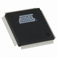
AT91SAM7XC128B-AU-999 Atmel, AT91SAM7XC128B-AU-999 Datasheet - Page 21

AT91SAM7XC128B-AU-999
Manufacturer Part Number
AT91SAM7XC128B-AU-999
Description
IC MCU ARM7 128KB FLASH 100LQFP
Manufacturer
Atmel
Series
AT91SAMr
Datasheet
1.AT91SAM7XC128B-CU.pdf
(47 pages)
Specifications of AT91SAM7XC128B-AU-999
Core Processor
ARM7
Core Size
16/32-Bit
Speed
55MHz
Connectivity
CAN, Ethernet, I²C, SPI, SSC, UART/USART, USB
Peripherals
Brown-out Detect/Reset, DMA, POR, PWM, WDT
Number Of I /o
62
Program Memory Size
128KB (128K x 8)
Program Memory Type
FLASH
Ram Size
32K x 8
Voltage - Supply (vcc/vdd)
1.65 V ~ 1.95 V
Data Converters
A/D 8x10b
Oscillator Type
Internal
Operating Temperature
-40°C ~ 85°C
Package / Case
100-LQFP
Lead Free Status / RoHS Status
Lead free / RoHS Compliant
Eeprom Size
-
Available stocks
Company
Part Number
Manufacturer
Quantity
Price
8.5
8.5.1
8.5.2
6209DS–ATARM–17-Feb-09
Embedded Flash
Flash Overview
Embedded Flash Controller
Figure 8-3.
The Flash contains a 256-byte write buffer, accessible through a 32-bit interface.
The Flash benefits from the integration of a power reset cell and from the brownout detector.
This prevents code corruption during power supply changes, even in the worst conditions.
When Flash is not used (read or write access), it is automatically placed into standby mode.
The Embedded Flash Controller (EFC) manages accesses performed by the masters of the sys-
tem. It enables reading the Flash and writing the write buffer. It also contains a User Interface,
mapped within the Memory Controller on the APB. The User Interface allows:
The Embedded Flash Controller also provides a dual 32-bit Prefetch Buffer that optimizes 16-bit
access to the Flash. This is particularly efficient when the processor is running in Thumb mode.
Two EFCs are embedded in the AT91SAM7XC512 to control each bank of 256 KBytes. Dual-
plane organization allows concurrent read and program functionality. Read from one memory
• The Flash of the AT91SAM7XC512 is organized in two banks (dual plane) 0f 1254 pages of
• The Flash of the AT91SAM7XC256 is organized in 1024 pages of 256 bytes (single plane). It
• The Flash of the AT91SAM7XC128 is organized in 512 pages of 256 bytes (single plane). It
• programming of the access parameters of the Flash (number of wait states, timings, etc.)
• starting commands such as full erase, page erase, page program, NVM bit set, NVM bit
• getting the end status of the last command
• getting error status
• programming interrupts on the end of the last commands or on errors
256 bytes. The 524, 288 bytes are organized in 32-bit words.
reads as 65,536 32-bit words.
reads as 32,768 32-bit words.
clear, etc.
256M Bytes
Internal Memory Mapping with GPNVM Bit 2 = 1
AT91SAM7XC512/256/128 Preliminary
0x0000 0000
0x0010 0000
0x0020 0000
0x0030 0000
0x000F FFFF
0x001F FFFF
0x002F FFFF
0x0FFF FFFF
0x003F FFFF
0x0040 0000
Flash Before Remap
SRAM After Remap
Undefined Areas
Internal FLASH
Internal SRAM
Internal ROM
(Abort)
252 M Bytes
1 M Bytes
1 M Bytes
1 M Bytes
1 M Bytes
21


