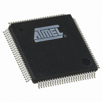
AT91SAM7XC128B-AU-999 Atmel, AT91SAM7XC128B-AU-999 Datasheet - Page 46

AT91SAM7XC128B-AU-999
Manufacturer Part Number
AT91SAM7XC128B-AU-999
Description
IC MCU ARM7 128KB FLASH 100LQFP
Manufacturer
Atmel
Series
AT91SAMr
Datasheet
1.AT91SAM7XC128B-CU.pdf
(47 pages)
Specifications of AT91SAM7XC128B-AU-999
Core Processor
ARM7
Core Size
16/32-Bit
Speed
55MHz
Connectivity
CAN, Ethernet, I²C, SPI, SSC, UART/USART, USB
Peripherals
Brown-out Detect/Reset, DMA, POR, PWM, WDT
Number Of I /o
62
Program Memory Size
128KB (128K x 8)
Program Memory Type
FLASH
Ram Size
32K x 8
Voltage - Supply (vcc/vdd)
1.65 V ~ 1.95 V
Data Converters
A/D 8x10b
Oscillator Type
Internal
Operating Temperature
-40°C ~ 85°C
Package / Case
100-LQFP
Lead Free Status / RoHS Status
Lead free / RoHS Compliant
Eeprom Size
-
Available stocks
Company
Part Number
Manufacturer
Quantity
Price
Revision History
Table 13-1.
46
Doc. Rev
6209S
6209BS
6209CS
6209DS
AT91SAM7XC512/256/128 Preliminary
Comments
First issue - Unqualified on Intranet
Legal page updated.Qualified on Intranet
Added AT91SAM7XC512 to product
Reformatted Memories
Reordered sub sections in Peripherals
Consolidated Memory Mapping in
Added package drawings
Consolidated Memory Mapping in
Added TFBGA information
page 10
Added LQFP and TFBGA package drawings
System Controller block diagram
“Features”, TWI updated to include Atmel TWI compatibility with I
“Features”,
Section 10.8 ”Two-wire
Section 10.11 ”Timer
Section 10.17 ”Analog-to-Digital
Figure 3-1,”Signal Description
Section 6.1 ”JTAG Port
Figure 9-1,”System Controller Block
Figure 8-1,”AT91SAM7XC512/256/128 Memory
Section 8.4.3 ”Internal
the Remap Command.”
Section 12. ”AT91SAM7XC512/256/128 Ordering
information.
Revision History
and
“Debug Unit (DBGU)”
“Features” on page 1
≤
Counter”,The TC has Two output compare or one input capture per channel.
Flash”,updated: “At any time, the Flash is mapped ... if GPNVM bit 2 is set and before
Section 8. “Memory” on page
Interface”, updated.
Pins”,
Section 11. “Package Drawings” on page
Section 4.3 “100-ball TFBGA Package Outline” on page
Section 6.2 ”Test Pin”
List”, footnote added to JTAGSEL, ERASE and TST pin comments
Converter”,INL and DNL updated.
Figure 9-1 on page
added
Figure 8-1 on page
Figure 8-1 on page
Diagram”, RTT is reset by power_on_reset.
family.“Features” on page 1
Section 10. “Peripherals” on page 32
“Mode for General Purpose 2-wire UART Serial
Section 11. on page
Mapping”,TDES base address is 0xFFFA 8000
Information”, MLR B chip revision added to ordering
and
26, “ice_nreset” signals changed to “power_on_reset”.
18.
19.
19.
Section 6.4 ”ERASE
and global
2
42.
C Standard.
42.
Pin”updated.
11. and
Communication”.
Section 4.4 on
6209DS–ATARM–17-Feb-09
Change
Request
Ref.
2729
4247
5846
4211
4008
5068
5225
5257
5850
6064


