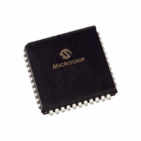
PIC16LC74B-04/L Microchip Technology, PIC16LC74B-04/L Datasheet - Page 79

PIC16LC74B-04/L
Manufacturer Part Number
PIC16LC74B-04/L
Description
IC MCU OTP 4KX14 A/D PWM 44PLCC
Manufacturer
Microchip Technology
Series
PIC® 16Cr
Specifications of PIC16LC74B-04/L
Core Processor
PIC
Core Size
8-Bit
Speed
4MHz
Connectivity
I²C, SPI, UART/USART
Peripherals
Brown-out Detect/Reset, POR, PWM, WDT
Number Of I /o
33
Program Memory Size
7KB (4K x 14)
Program Memory Type
OTP
Ram Size
192 x 8
Voltage - Supply (vcc/vdd)
2.5 V ~ 5.5 V
Data Converters
A/D 5x8b
Oscillator Type
External
Operating Temperature
0°C ~ 70°C
Package / Case
44-PLCC
Lead Free Status / RoHS Status
Lead free / RoHS Compliant
Eeprom Size
-
Available stocks
Company
Part Number
Manufacturer
Quantity
Price
Company:
Part Number:
PIC16LC74B-04/L
Manufacturer:
MICROCHIP
Quantity:
6 237
Company:
Part Number:
PIC16LC74B-04/L
Manufacturer:
Microchip Technology
Quantity:
10 000
12.0
The 8-bit Analog-to-Digital (A/D) converter module has
five inputs for the PIC16C73B and eight for the
PIC16C74B.
The A/D allows conversion of an analog input signal to
a corresponding 8-bit digital number. The output of the
sample and hold is the input into the converter, which
generates the result via successive approximation. The
analog reference voltage is software selectable to
either the device’s positive supply voltage (V
voltage level on the RA3/AN3/V
REGISTER 12-1:
Note:
2000 Microchip Technology Inc.
ANALOG-TO-DIGITAL
CONVERTER (A/D) MODULE
bit 7-6
bit 5-3
bit 2
bit 1
bit 0
The PIC16C63A and PIC16C65B do not
include A/D modules. ADCON0, ADCON1
and ADRES registers are not imple-
mented. ADIF and ADIE bits are reserved
and should be maintained clear.
ADCON0 REGISTER (ADDRESS 1Fh)
ADCS1:ADCS0: A/D Conversion Clock Select bits
00 = F
01 = F
10 = F
11 = F
CHS2:CHS0: Analog Channel Select bits
000 = channel 0, (RA0/AN0)
001 = channel 1, (RA1/AN1)
010 = channel 2, (RA2/AN2)
011 = channel 3, (RA3/AN3)
100 = channel 4, (RA5/AN4)
101 = channel 5, (RE0/AN5)
110 = channel 6, (RE1/AN6)
111 = channel 7, (RE2/AN7)
GO/DONE: A/D Conversion Status bit
If ADON = 1:
1 = A/D conversion in progress (setting this bit starts the A/D conversion)
0 = A/D conversion not in progress (this bit is automatically cleared by hardware when the A/D
Unimplemented: Read as '0'
ADON: A/D On bit
1 = A/D converter module is operating
0 = A/D converter module is shut-off and consumes no operating current
Note 1: A/D channels 5, 6 and 7 are implemented on the PIC16C74B only.
bit 7
Legend:
R = Readable bit
-n = Value at POR
ADCS1
R/W-0
conversion is complete)
OSC
OSC
OSC
RC
REF
(clock derived from the internal A/D module RC oscillator)
/2
/8
/32
pin.
ADCS0
R/W-0
DD
), or the
R/W-0
CHS2
W = Writable bit
’1’ = Bit is set
(1)
(1)
(1)
PIC16C63A/65B/73B/74B
R/W-0
CHS1
The A/D converter has a unique feature of being able
to operate while the device is in SLEEP mode. To oper-
ate in SLEEP, the A/D conversion clock must be
derived from the A/D’s internal RC oscillator.
The A/D module has three registers. These registers
are:
• A/D Result Register (ADRES)
• A/D Control Register 0 (ADCON0)
• A/D Control Register 1 (ADCON1)
The ADCON0 register, shown in Register 12-1, con-
trols the operation of the A/D module. The ADCON1
register, shown in Register 12-2, configures the func-
tions of the port pins. The port pins can be configured
as analog inputs (RA3 can also be a voltage reference),
or as digital I/O.
Additional information on using the A/D module can be
found in the PICmicro™ Mid-Range MCU Family Ref-
erence Manual (DS33023) and in Application Note,
AN546.
R/W-0
CHS0
U = Unimplemented bit, read as ‘0’
’0’ = Bit is cleared
GO/DONE
R/W-0
x = Bit is unknown
U-0
—
DS30605C-page 79
ADON
R/W-0
bit 0


