AT91SAM7SE32-CU-999 Atmel, AT91SAM7SE32-CU-999 Datasheet
AT91SAM7SE32-CU-999
Specifications of AT91SAM7SE32-CU-999
Available stocks


Related parts for AT91SAM7SE32-CU-999


AT91SAM7SE32-CU-999 Summary of contents
Page 1
... Plane (AT91SAM7SE512) – 256 Kbytes (AT91SAM7SE256) Organized in One Bank of 1024 Pages of 256 Bytes Single Plane (AT91SAM7SE256) – 32 Kbytes (AT91SAM7SE32) Organized in One Bank of 256 Pages of 128 Bytes Single Plane (AT91SAM7SE32) – Single Cycle Access MHz in Worst Case Conditions – Prefetch Buffer Optimizing Thumb Instruction Execution at Maximum Speed – ...
Page 2
... One Four-channel 16-bit PWM Controller (PWMC) • One Two-wire Interface (TWI) – Master, Multi-Master and Slave Mode Support, All Two-wire Atmel EEPROMs Supported – General Call Supported in Slave Mode • One 8-channel 10-bit Analog-to-Digital Converter, Four Channels Multiplexed with Digital I/Os ® ...
Page 3
... AT91SAM7SE512 features a 512 Kbyte high-speed Flash and a 32 Kbyte SRAM. • AT91SAM7SE256 features a 256 Kbyte high-speed Flash and a 32 Kbyte SRAM. • AT91SAM7SE32 features a 32 Kbyte high-speed Flash and an 8 Kbyte SRAM. It also embeds a large set of peripherals, including a USB 2.0 device, an External Bus Interface (EBI), and a complete set of system functions minimizing the number of external components ...
Page 4
Block Diagram Figure 2-1. JTAGSEL IRQ0-IRQ1 DRXD DTXD PCK0-PCK2 PLLRC XOUT VDDFLASH VDDCORE VDDCORE NRST RXD0 SCK0 RXD1 SCK1 DCD1 DSR1 DTR1 NPCS0 NPCS1 NPCS2 NPCS3 SPCK TCLK0 TCLK1 TCLK2 TIOA0 TIOB0 TIOA1 TIOB1 TIOA2 TIOB2 ADTRG ADVREF AT91SAM7SE512/256/32 ...
Page 5
AT91SAM7SE512/256/32 Preliminary Summary 3. Signal Description Table 3-1. Signal Description List Signal Name Function Voltage Regulator and ADC Power VDDIN Supply Input VDDOUT Voltage Regulator Output VDDFLASH Flash and USB Power Supply VDDIO I/O Lines Power Supply VDDCORE Core Power ...
Page 6
Table 3-1. Signal Description List (Continued) Signal Name Function PA0 - PA31 Parallel IO Controller A PB0 - PB31 Parallel IO Controller B PC0 - PC23 Parallel IO Controller C DDM USB Device Port Data - DDP USB Device Port ...
Page 7
AT91SAM7SE512/256/32 Preliminary Summary Table 3-1. Signal Description List (Continued) Signal Name Function TWD Two-wire Serial Data TWCK Two-wire Serial Clock AD0-AD3 Analog Inputs AD4-AD7 Analog Inputs ADTRG ADC Trigger ADVREF ADC Reference PGMEN0-PGMEN2 Programming Enabling PGMM0-PGMM3 Programming Mode PGMD0-PGMD15 Programming ...
Page 8
Table 3-1. Signal Description List (Continued) Signal Name Function NANDCS NAND Flash Chip Select Line NANDOE NAND Flash Output Enable NANDWE NAND Flash Write Enable NANDCLE NAND Flash Command Line Enable NANDALE NAND Flash Address Line Enable SDCK SDRAM Clock ...
Page 9
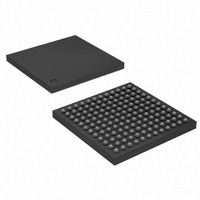
AT91SAM7SE512/256/32 Preliminary Summary 4. Package The AT91SAM7SE512/256/32 is available in: • 128-lead LQFP package with a 0.5 mm lead pitch. • 10x 10 x 1.4 mm 144-ball LFBGA package with a 0.8 mm lead pitch 4.1 ...
Page 10
LQFP Pinout Table 4-1. Pinout in 128-lead LQFP Package 1 ADVREF 33 2 GND 34 3 AD7 35 4 AD6 36 5 AD5 37 6 AD4 38 7 VDDOUT 39 8 VDDIN 40 9 PA20/PGMD8/AD3 41 10 PA19/PGMD7/AD2 ...
Page 11
AT91SAM7SE512/256/32 Preliminary Summary 4.3 144-ball LFBGA Package Outline Figure 4-2 description is given in the Mechanical Characteristics section. Figure 4-2. 6222ES–ATARM–15-Dec-09 shows the orientation of the 144-ball LFBGA package and a detailed mechanical 144-ball LFBGA Package Outline (Top View) 12 ...
Page 12
LFBGA Pinout Table 4-2. SAM7SE512/256/32 Pinout for 144-ball LFBGA Package Pin Signal Name Pin A1 PB7 D1 A2 PB8 D2 A3 PB9 D3 A4 PB12 D4 A5 PB13 D5 A6 PB16 D6 A7 PB22 D7 A8 PB23 D8 ...
Page 13
AT91SAM7SE512/256/32 Preliminary Summary 5. Power Considerations 5.1 Power Supplies The AT91SAM7SE512/256/32 has six types of power supply pins and integrates a voltage regu- lator, allowing the device to be supplied with only one voltage. The six power supply pin types ...
Page 14
One external 470 pF (or 1 nF) NPO capacitor should be connected between VDDOUT and GND as close to the chip as possible. • One external 2.2 µF (or 3.3 µF) X7R capacitor should be connected between VDDOUT and ...
Page 15
AT91SAM7SE512/256/32 Preliminary Summary 6. /O Lines Considerations 6.1 JTAG Port Pins TMS, TDI and TCK are Schmitt trigger inputs. TMS, TDI and TCK do not integrate a pull-up resistor. TDO is an output, driven VDDIO, and has ...
Page 16
SDCK Pin The SDCK pin is dedicated to the SDRAM Clock and is an output-only without pull-up. Maximum Output Frequency of this pad is 48 MHz at 3.0V and 25 MHz at 1.65V with a maximum load of 30 ...
Page 17
AT91SAM7SE512/256/32 Preliminary Summary 7. Processor and Architecture 7.1 ARM7TDMI Processor • RISC processor based on ARMv4T Von Neumann architecture – Runs MHz, providing 0.9 MIPS/MHz (core supplied with 1.8V) • Two instruction sets – ARM – ...
Page 18
Individually programmable size between 1K Byte and 1M Byte – Individually programmable protection against write and/or user access – Peripheral protection against write and/or user access • Embedded Flash Controller – Embedded Flash interface three programmable wait ...
Page 19
AT91SAM7SE512/256/32 Preliminary Summary • Multiple device adaptability – Compliant with LCD Module – Compliant with PSRAM in synchronous operations – Programmable Setup Time Read/Write – Programmable Hold Time Read/Write • Multiple Wait State Management – Programmable Wait State Generation – ...
Page 20
Peripheral DMA Controller • Handles data transfer between peripherals and memories • Eleven channels – Two for each USART – Two for the Debug Unit – Two for the Serial Synchronous Controller – Two for the Serial Peripheral Interface ...
Page 21
... Protection Mode to secure contents of the Flash • 32 Kbytes of Fast SRAM (AT91SAM7SE512/256) – Single-cycle access at full speed • 8 Kbytes of Fast SRAM (AT91SAM7SE32) – Single-cycle access at full speed 6222ES–ATARM–15-Dec-09 21 ...
Page 22
Figure 8-1. AT91SAM7SE Memory Mapping Address Memory Space 0x0000 0000 Internal Memories 256 MBytes 0x0FFF FFFF 0x1000 0000 EBI Chip Select 0 256 MBytes SMC 0x1FFF FFFF 0x2000 0000 EBI 256 MBytes Chip Select 1/ SMC or SDRAMC 0x2FFF FFFF ...
Page 23
... The AT91SAM7SE512 features two banks of 256 Kbytes of Flash. • The AT91SAM7SE256 features one bank of 256 Kbytes of Flash. • The AT91SAM7SE32 features one bank of 32 Kbytes of Flash. At any time, the Flash is mapped to address 0x0010 0000. A general purpose NVM (GPNVM) bit is used to boot either on the ROM (default) or from the Flash. This GPNVM bit can be cleared or set respectively through the commands “ ...
Page 24
... The Flash of the AT91SAM7SE256 is organized in 1024 pages (single plane) of 256 bytes. It reads as 65,536 32-bit words. The Flash of the AT91SAM7SE32 is organized in 256 pages (single plane) of 128 bytes. It reads as 8192 32-bit words. The Flash of the AT91SAM7SE32 contains a 128-byte write buffer, accessible through a 32-bit interface ...
Page 25
... AT91SAM7SE256 contains 16 lock regions and each lock region contains 64 pages of 256 bytes. Each lock region has a size of 16 Kbytes. The AT91SAM7SE32 Embedded Flash Controller manages 8 lock bits to protect 8 regions of the flash against inadvertent flash erasing or programming commands. The AT91SAM7SE32 contains 8 lock regions and each lock region contains 32 pages of 128 bytes. Each lock region has a size of 4 Kbytes locked-region’ ...
Page 26
... The Flash of the AT91SAM7SE256 is organized in 1024 pages of 256 bytes (single plane). It reads as 65,536 32-bit words. • The Flash of the AT91SAM7SE32 is organized in 256 pages of 128 bytes (single plane). It reads as 32,768 32-bit words. • The Flash of the AT91SAM7SE512/256 contains a 256-byte write buffer, accessible through a 32-bit interface. • ...
Page 27
AT91SAM7SE512/256/32 Preliminary Summary ® 8.1.4 SAM-BA Boot The SAM-BA Boot is a default Boot Program which provides an easy way to program in-situ the on-chip Flash memory. The SAM-BA Boot Assistant supports serial communication via the DBGU or the USB ...
Page 28
System Controller The System Controller manages all vital blocks of the microcontroller: interrupts, clocks, power, time, debug and reset. The System Controller peripherals are all mapped to the highest 4 Kbytes of address space, between addresses 0xFFFF F000 and ...
Page 29
AT91SAM7SE512/256/32 Preliminary Summary Figure 9-1. NRST XOUT PLLRC PA0-PA31 PB0-PB31 PC0-PC29 6222ES–ATARM–15-Dec-09 System Controller Block Diagram System Controller irq0-irq1 Advanced fiq Interrupt Controller periph_irq[2..18] pit_irq rtt_irq wdt_irq dbgu_irq pmc_irq rstc_irq MCK Debug periph_nreset Unit dbgu_rxd Periodic MCK debug Interval periph_nreset ...
Page 30
Reset Controller • Based on one power-on reset cell and a double brownout detector • Status of the last reset, either Power-up Reset, Software Reset, User Reset, Watchdog Reset, Brownout Reset • Controls the internal resets and the NRST ...
Page 31
AT91SAM7SE512/256/32 Preliminary Summary • Main Oscillator frequency ranges between 3 and 20 MHz • Main Oscillator can be bypassed • PLL output ranges between 80 and 220 MHz It provides SLCK, MAINCK and PLLCK. Figure 9-2. 9.3 Power Management Controller ...
Page 32
Figure 9-3. 9.4 Advanced Interrupt Controller • Controls the interrupt lines (nIRQ and nFIQ ARM Processor • Individually maskable and vectored interrupt sources – Source 0 is reserved for the Fast Interrupt Input (FIQ) – Source 1 is ...
Page 33
... Identification of the device revision, sizes of the embedded memories, set of – Chip ID is 0x272A 0A40 (VERSION 0) for AT91SAM7SE512 – Chip ID is 0x272A 0940 (VERSION 0) for AT91SAM7SE256 – Chip ID is 0x2728 0340 (VERSION 0) for AT91SAM7SE32 9.6 Periodic Interval Timer • 20-bit programmable counter plus 12-bit interval counter 9 ...
Page 34
Synchronous output, provides Set and Clear of several I/O lines in a single write 9.10 Voltage Regulator Controller The purpose of this controller is to select the Power Mode of the Voltage Regulator between Normal Mode (bit 0 is ...
Page 35
AT91SAM7SE512/256/32 Preliminary Summary 10. Peripherals 10.1 User Interface The User Peripherals are mapped in the 256 MBytes of the address space between 0xF000 0000 and 0xFFFF EFFF. Each peripheral is allocated 16 Kbytes of address space. A complete memory map ...
Page 36
Peripheral Multiplexing on PIO Lines The AT91SAM7SE512/256/32 features three PIO controllers, PIOA, PIOB and PIOC, that multi- plex the I/O lines of the peripheral set. PIO Controller A and B control 32 lines; PIO Controller C controls 24 lines. ...
Page 37
AT91SAM7SE512/256/32 Preliminary Summary 10.4 PIO Controller A Multiplexing Table 10-2. Multiplexing on PIO Controller A PIO Controller A I/O Line Peripheral A PA0 PWM0 PA1 PWM1 PA2 PWM2 PA3 TWD PA4 TWCK PA5 RXD0 PA6 TXD0 PA7 RTS0 PA8 CTS0 ...
Page 38
PIO Controller B Multiplexing Table 10-3. Multiplexing on PIO Controller B PIO Controller B I/O Line Peripheral A PB0 TIOA0 PB1 TIOB0 PB2 SCK0 PB3 NPCS3 PB4 TCLK0 PB5 NPCS3 PB6 PCK0 PB7 PWM3 PB8 ADTRG PB9 NPCS1 PB10 ...
Page 39
AT91SAM7SE512/256/32 Preliminary Summary 10.6 PIO Controller C Multiplexing Multiplexing on PIO Controller C PIO Controller C I/O Line Peripheral A PC0 D0 PC1 D1 PC2 D2 PC3 D3 PC4 D4 PC5 D5 PC6 D6 PC7 D7 PC8 D8 PC9 D9 ...
Page 40
Programmable phase and polarity per chip select – Programmable transfer delays per chip select, between consecutive transfers and between clock and data – Programmable delay between consecutive transfers – ...
Page 41
AT91SAM7SE512/256/32 Preliminary Summary • Offers a configurable frame sync and data length • Receiver and transmitter can be programmed to start automatically or on detection of different event on the frame sync signal • Receiver and transmitter include a data ...
Page 42
USB Device Port • USB V2.0 full-speed compliant,12 Mbits per second. • Embedded USB V2.0 full-speed transceiver • Embedded 2688-byte dual-port RAM for endpoints • Eight endpoints – Endpoint 0: 64bytes – Endpoint 1 and 2: 64 bytes ping-pong ...
Page 43
AT91SAM7SE512/256/32 Preliminary Summary 11. Package Drawings Figure 11-1. 128-lead LQFP Package Drawing 6222ES–ATARM–15-Dec-09 43 ...
Page 44
Figure 11-2. 144-ball LFBGA Package Drawing All dimensions are in mm AT91SAM7SE512/256/32 Preliminary 44 6222ES–ATARM–15-Dec-09 ...
Page 45
... AT91SAM7SE512/256/32 Preliminary Summary 12. Ordering Information Table 12-1. Ordering Information Ordering Code AT91SAM7SE512-AU AT91SAM7SE256-AU AT91SAM7SE32-AU AT91SAM7SE512-CU AT91SAM7SE256-CU AT91SAM7SE32-CU 6222ES–ATARM–15-Dec-09 Package Package Type LQFP128 Green LQFP128 Green LQFP128 Green LFBGA144 Green LFBGA144 Green LFBGA144 Green Temperature Operating Range Industrial (-40° 85° C) Industrial (-40° ...
Page 46
... Section 7.5 ”Static Memory synchronous operations. Figure 8-1 ”AT91SAM7SE Memory Mapping” shown with EBI Chip Select 2. 6222DS Section 8.1.2.1 ”Flash Overview”, updated AT91SAM7SE32 ...”reads as 8192 32-bit words.” Section 6. ”/O Lines Considerations”, updated 6222ES Section 10.11 ”Timer Counter”, .....the TC has two output compare and one input capture per channel. ...
Page 47
... Disclaimer: The information in this document is provided in connection with Atmel products. No license, express or implied, by estoppel or otherwise, to any intellectual property right is granted by this document or in connection with the sale of Atmel products. EXCEPT AS SET FORTH IN ATMEL’S TERMS AND CONDI- TIONS OF SALE LOCATED ON ATMEL’S WEB SITE, ATMEL ASSUMES NO LIABILITY WHATSOEVER AND DISCLAIMS ANY EXPRESS, IMPLIED OR STATUTORY WARRANTY RELATING TO ITS PRODUCTS INCLUDING, BUT NOT LIMITED TO, THE IMPLIED WARRANTY OF MERCHANTABILITY, FITNESS FOR A PARTICULAR PURPOSE, OR NON-INFRINGEMENT ...