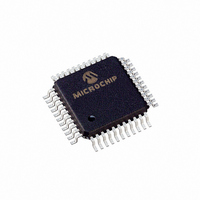
PIC16LC74B-04I/PQ Microchip Technology, PIC16LC74B-04I/PQ Datasheet - Page 19

PIC16LC74B-04I/PQ
Manufacturer Part Number
PIC16LC74B-04I/PQ
Description
IC MCU OTP 4KX14 A/D PWM 44-MQFP
Manufacturer
Microchip Technology
Series
PIC® 16Cr
Specifications of PIC16LC74B-04I/PQ
Core Processor
PIC
Core Size
8-Bit
Speed
4MHz
Connectivity
I²C, SPI, UART/USART
Peripherals
Brown-out Detect/Reset, POR, PWM, WDT
Number Of I /o
33
Program Memory Size
7KB (4K x 14)
Program Memory Type
OTP
Ram Size
192 x 8
Voltage - Supply (vcc/vdd)
2.5 V ~ 5.5 V
Data Converters
A/D 5x8b
Oscillator Type
External
Operating Temperature
-40°C ~ 85°C
Package / Case
44-MQFP, 44-PQFP
Processor Series
PIC16LC
Core
PIC
Data Bus Width
8 bit
Data Ram Size
192 B
Interface Type
I2C, SPI, USART
Maximum Clock Frequency
4 MHz
Number Of Programmable I/os
33
Number Of Timers
8
Operating Supply Voltage
2.5 V to 5.5 V
Maximum Operating Temperature
+ 85 C
Mounting Style
SMD/SMT
3rd Party Development Tools
52715-96, 52716-328, 52717-734
Development Tools By Supplier
ICE2000, DM163022
Minimum Operating Temperature
- 40 C
On-chip Adc
8
Lead Free Status / RoHS Status
Lead free / RoHS Compliant
Eeprom Size
-
Lead Free Status / Rohs Status
Details
Available stocks
Company
Part Number
Manufacturer
Quantity
Price
Company:
Part Number:
PIC16LC74B-04I/PQ
Manufacturer:
Microchip Technology
Quantity:
10 000
4.2.2.1
The STATUS register, shown in Register 4-1, contains
the arithmetic status of the ALU, the RESET status and
the bank select bits for data memory.
The STATUS register can be the destination for any
instruction, as with any other register. If the STATUS reg-
ister is the destination for an instruction that affects the Z,
DC or C bits, then the write to these three bits is disabled.
These bits are set or cleared according to the device
logic. Furthermore, the TO and PD bits are not writable.
Therefore, the result of an instruction with the STATUS
register as destination may be different than intended.
For example, CLRF STATUS will clear the upper three
bits and set the Z bit. This leaves the STATUS register
as 000u u1uu (where u = unchanged).
REGISTER 4-1:
2000 Microchip Technology Inc.
bit 7
bit 6-5
bit 4
bit 3
bit 2
bit 1
bit 0
STATUS Register
STATUS REGISTER (ADDRESS 03h, 83h)
bit 7
IRP
1 = Bank 2, 3 (100h - 1FFh)
0 = Bank 0, 1 (00h - FFh)
RP1
11 = Bank 3 (180h - 1FFh)
10 = Bank 2 (100h - 17Fh)
01 = Bank 1 (80h - FFh)
00 = Bank 0 (00h - 7Fh)
Each bank is 128 bytes
TO: Time-out bit
1 = After power-up, CLRWDT instruction, or SLEEP instruction
0 = A WDT time-out occurred
PD: Power-down bit
1 = After power-up or by the CLRWDT instruction
0 = By execution of the SLEEP instruction
Z: Zero bit
1 = The result of an arithmetic or logic operation is zero
0 = The result of an arithmetic or logic operation is not zero
DC: Digit carry/borrow bit (ADDWF,ADDLW,SUBLW,SUBWF instructions) (for borrow the polarity
is reversed)
1 = A carry-out from the 4th low order bit of the result occurred
0 = No carry-out from the 4th low order bit of the result
C
1 = A carry-out from the most significant bit of the result occurred
0 = No carry-out from the most significant bit of the result occurred
Note 1: Maintain the IRP and RP1 bits clear.
Legend:
R = Readable bit
-n = Value at POR
(2)
R/W-0
IRP
(1)
: Carry/borrow bit (ADDWF,ADDLW,SUBLW,SUBWF instructions)
(1)
(1)
: Register Bank Select bit (used for indirect addressing)
2: For borrow and digit borrow, the polarity is reversed. A subtraction is executed by
:RP0: Register Bank Select bits (used for direct addressing)
adding the two’s complement of the second operand. For rotate (RRF,RLF) instruc-
tions, this bit is loaded with either the high or low order bit of the source register.
RP1
R/W-0
(1)
R/W-0
RP0
W = Writable bit
’1’ = Bit is set
PIC16C63A/65B/73B/74B
It is recommended that only BCF, BSF, SWAPF and
MOVWF instructions be used to alter the STATUS regis-
ter. These instructions do not affect the Z, C or DC bits
in the STATUS register. For other instructions which do
not affect status bits, see the "Instruction Set Sum-
mary."
R-1
TO
Note 1: These devices do not use bits IRP and
2: The C and DC bits operate as borrow and
U = Unimplemented bit, read as ‘0’
’0’ = Bit is cleared
RP1 (STATUS<7:6>), maintain these bits
clear to ensure upward compatibility with
future products.
digit borrow bits, respectively, in subtrac-
tion. See the SUBLW and SUBWF instruc-
tions for examples.
R-1
PD
R/W-x
Z
x = Bit is unknown
R/W-x
DC
DS30605C-page 19
R/W-x
C
(2)
bit 0


