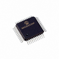
PIC16LC74B-04I/PQ Microchip Technology, PIC16LC74B-04I/PQ Datasheet - Page 53

PIC16LC74B-04I/PQ
Manufacturer Part Number
PIC16LC74B-04I/PQ
Description
IC MCU OTP 4KX14 A/D PWM 44-MQFP
Manufacturer
Microchip Technology
Series
PIC® 16Cr
Specifications of PIC16LC74B-04I/PQ
Core Processor
PIC
Core Size
8-Bit
Speed
4MHz
Connectivity
I²C, SPI, UART/USART
Peripherals
Brown-out Detect/Reset, POR, PWM, WDT
Number Of I /o
33
Program Memory Size
7KB (4K x 14)
Program Memory Type
OTP
Ram Size
192 x 8
Voltage - Supply (vcc/vdd)
2.5 V ~ 5.5 V
Data Converters
A/D 5x8b
Oscillator Type
External
Operating Temperature
-40°C ~ 85°C
Package / Case
44-MQFP, 44-PQFP
Processor Series
PIC16LC
Core
PIC
Data Bus Width
8 bit
Data Ram Size
192 B
Interface Type
I2C, SPI, USART
Maximum Clock Frequency
4 MHz
Number Of Programmable I/os
33
Number Of Timers
8
Operating Supply Voltage
2.5 V to 5.5 V
Maximum Operating Temperature
+ 85 C
Mounting Style
SMD/SMT
3rd Party Development Tools
52715-96, 52716-328, 52717-734
Development Tools By Supplier
ICE2000, DM163022
Minimum Operating Temperature
- 40 C
On-chip Adc
8
Lead Free Status / RoHS Status
Lead free / RoHS Compliant
Eeprom Size
-
Lead Free Status / Rohs Status
Details
Available stocks
Company
Part Number
Manufacturer
Quantity
Price
Company:
Part Number:
PIC16LC74B-04I/PQ
Manufacturer:
Microchip Technology
Quantity:
10 000
A PWM output (Figure 9-4) has a time-base (period)
and a time that the output stays high (duty cycle). The
frequency of the PWM is the inverse of the period
(1/period).
FIGURE 9-4:
9.3.1
The PWM period is specified by writing to the PR2
register. The PWM period can be calculated using the
following formula:
PWM frequency is defined as 1 / [PWM period].
When TMR2 is equal to PR2, the following three events
occur on the next increment cycle:
• TMR2 is cleared
• The CCP1 pin is set (exception: if PWM duty
• The PWM duty cycle is latched from CCPR1L into
TABLE 9-3:
cycle = 0%, the CCP1 pin will not be set)
CCPR1H
Note:
2000 Microchip Technology Inc.
PWM period = [(PR2) + 1] • 4 • T
TMR2 = PR2
Maximum Resolution (bits)
Timer Prescaler (1, 4, 16)
Duty Cycle
The Timer2 postscaler (see Section 8.1) is
not used in the determination of the PWM
frequency. The postscaler could be used to
have a servo update rate at a different fre-
quency than the PWM output.
PWM PERIOD
PWM Frequency
Period
PR2 Value
EXAMPLE PWM FREQUENCIES AND RESOLUTIONS AT 20 MHz
TMR2 = Duty Cycle
(TMR2 prescale value)
(Timer2 RESET)
PWM OUTPUT
TMR2 = PR2 (Timer2 RESET)
OSC
•
1.22 kHz 4.88 kHz 19.53 kHz 78.12 kHz 156.3 kHz 208.3 kHz
0xFF
16
10
PIC16C63A/65B/73B/74B
0xFF
10
4
9.3.2
The PWM duty cycle is specified by writing to the
CCPR1L register and to the CCP1CON<5:4> bits. Up
to 10-bit resolution is available: the CCPR1L contains
the eight MSbs and the CCP1CON<5:4> contains the
two LSbs. This 10-bit value is represented by
CCPR1L:CCP1CON<5:4>. The following equation is
used to calculate the PWM duty cycle in time:
CCPR1L and CCP1CON<5:4> can be written to at any
time, but the duty cycle value is not latched into
CCPR1H until after a match between PR2 and TMR2
occurs (i.e., the period is complete). In PWM mode,
CCPR1H is a read-only register.
The CCPR1H register and a 2-bit internal latch are
used to double buffer the PWM duty cycle. This double
buffering is essential for glitchless PWM operation.
When the CCPR1H and 2-bit latch match TMR2, con-
catenated with an internal 2-bit Q clock, or 2 bits of the
TMR2 prescaler, the CCP1 pin is cleared.
Maximum PWM resolution (bits) for a given PWM
frequency:
9.3.3
The following steps should be taken when configuring
the CCP module for PWM operation:
1.
2.
3.
4.
5.
Note:
PWM duty cycle = (CCPR1L:CCP1CON<5:4>) •
Resolution
Set the PWM period by writing to the PR2 register.
Set the PWM duty cycle by writing to the
CCPR1L register and CCP1CON<5:4> bits.
Make the CCP1 pin an output by clearing the
TRISC<2> bit.
Set the TMR2 prescale value and enable Timer2
by writing to T2CON.
Configure the CCP1 module for PWM operation.
0xFF
10
1
If the PWM duty cycle value is longer than
the PWM period, the CCP1 pin will not be
cleared.
PWM DUTY CYCLE
SET-UP FOR PWM OPERATION
=
log
0x3F
T
1
8
OSC
(
log(2)
F
F
PWM
OSC
• (TMR2 prescale value)
)
0x1F
bits
1
7
DS30605C-page 53
0x17
5.5
1


