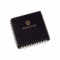
PIC16LF874A-I/L Microchip Technology, PIC16LF874A-I/L Datasheet - Page 131

PIC16LF874A-I/L
Manufacturer Part Number
PIC16LF874A-I/L
Description
IC MCU FLASH 4KX14 EE A/D 44PLCC
Manufacturer
Microchip Technology
Series
PIC® 16Fr
Specifications of PIC16LF874A-I/L
Core Size
8-Bit
Program Memory Size
7KB (4K x 14)
Core Processor
PIC
Speed
10MHz
Connectivity
I²C, SPI, UART/USART
Peripherals
Brown-out Detect/Reset, POR, PWM, WDT
Number Of I /o
33
Program Memory Type
FLASH
Eeprom Size
128 x 8
Ram Size
192 x 8
Voltage - Supply (vcc/vdd)
2 V ~ 5.5 V
Data Converters
A/D 8x10b
Oscillator Type
External
Operating Temperature
-40°C ~ 85°C
Package / Case
44-PLCC
Controller Family/series
PIC16LF
No. Of I/o's
33
Eeprom Memory Size
128Byte
Ram Memory Size
192Byte
Cpu Speed
20MHz
No. Of Timers
3
Lead Free Status / RoHS Status
Lead free / RoHS Compliant
Other names
PIC16LF874A-I/LR
PIC16LF874A-I/LR
PIC16LF874AI/L
PIC16LF874A-I/LR
PIC16LF874AI/L
Available stocks
Company
Part Number
Manufacturer
Quantity
Price
Company:
Part Number:
PIC16LF874A-I/L
Manufacturer:
Microchip Technology
Quantity:
10 000
Part Number:
PIC16LF874A-I/L
Manufacturer:
MIC
Quantity:
20 000
- Current page: 131 of 234
- Download datasheet (5Mb)
The ADRESH:ADRESL registers contain the 10-bit
result of the A/D conversion. When the A/D conversion
is complete, the result is loaded into this A/D Result
register pair, the GO/DONE bit (ADCON0<2>) is cleared
and the A/D interrupt flag bit ADIF is set. The block
diagram of the A/D module is shown in Figure 11-1.
After the A/D module has been configured as desired,
the selected channel must be acquired before the con-
version is started. The analog input channels must
have their corresponding TRIS bits selected as inputs.
To determine sample time, see Section 11.1 “A/D
Acquisition Requirements”. After this acquisition
time has elapsed, the A/D conversion can be started.
To do an A/D Conversion, follow these steps:
1.
FIGURE 11-1:
2003 Microchip Technology Inc.
Note 1: Not available on 28-pin devices.
Configure the A/D module:
• Configure analog pins/voltage reference and
• Select A/D input channel (ADCON0)
• Select A/D conversion clock (ADCON0)
• Turn on A/D module (ADCON0)
digital I/O (ADCON1)
Converter
A/D
A/D BLOCK DIAGRAM
(Reference
(Reference
Voltage)
Voltage)
V
V
REF
REF
-
+
(Input Voltage)
PCFG3:PCFG0
PCFG3:PCFG0
V
AIN
V
V
DD
SS
2.
3.
4.
5.
6.
7.
Configure A/D interrupt (if desired):
• Clear ADIF bit
• Set ADIE bit
• Set PEIE bit
• Set GIE bit
Wait the required acquisition time.
Start conversion:
• Set GO/DONE bit (ADCON0)
Wait for A/D conversion to complete by either:
• Polling for the GO/DONE bit to be cleared
• Waiting for the A/D interrupt
Read
(ADRESH:ADRESL), clear bit ADIF if required.
For the next conversion, go to step 1 or step 2
as required. The A/D conversion time per bit is
defined as T
(interrupts disabled); OR
CHS2:CHS0
A/D
AD
111
110
101
100
011
010
001
000
.
PIC16F87XA
Result
DS39582B-page 129
register
RA1/AN1
RE2/AN7
RA2/AN2/V
RA0/AN0
RE1/AN6
RE0/AN5
RA5/AN4
RA3/AN3/V
(1)
(1)
(1)
REF
REF
pair
+
-
Related parts for PIC16LF874A-I/L
Image
Part Number
Description
Manufacturer
Datasheet
Request
R

Part Number:
Description:
IC MCU FLASH 4KX14 EEPROM 18SOIC
Manufacturer:
Microchip Technology
Datasheet:

Part Number:
Description:
IC MCU FLASH 4KX14 EEPROM 18DIP
Manufacturer:
Microchip Technology
Datasheet:

Part Number:
Description:
IC MCU FLASH 4KX14 EEPROM 20SSOP
Manufacturer:
Microchip Technology
Datasheet:

Part Number:
Description:
(PIC16LF87 / PIC16LF88) 18/20/28-Pin Enhanced FLASH Microcontrollers with nanoWatt Technology
Manufacturer:
Microchip Technology

Part Number:
Description:
IC MCU FLASH 4KX14 EEPROM 28QFN
Manufacturer:
Microchip Technology
Datasheet:

Part Number:
Description:
Manufacturer:
Microchip Technology Inc.
Datasheet:

Part Number:
Description:
Manufacturer:
Microchip Technology Inc.
Datasheet:

Part Number:
Description:
Manufacturer:
Microchip Technology Inc.
Datasheet:

Part Number:
Description:
Manufacturer:
Microchip Technology Inc.
Datasheet:

Part Number:
Description:
Manufacturer:
Microchip Technology Inc.
Datasheet:

Part Number:
Description:
Manufacturer:
Microchip Technology Inc.
Datasheet:


