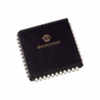
PIC16LF874A-I/L Microchip Technology, PIC16LF874A-I/L Datasheet - Page 139

PIC16LF874A-I/L
Manufacturer Part Number
PIC16LF874A-I/L
Description
IC MCU FLASH 4KX14 EE A/D 44PLCC
Manufacturer
Microchip Technology
Series
PIC® 16Fr
Specifications of PIC16LF874A-I/L
Core Size
8-Bit
Program Memory Size
7KB (4K x 14)
Core Processor
PIC
Speed
10MHz
Connectivity
I²C, SPI, UART/USART
Peripherals
Brown-out Detect/Reset, POR, PWM, WDT
Number Of I /o
33
Program Memory Type
FLASH
Eeprom Size
128 x 8
Ram Size
192 x 8
Voltage - Supply (vcc/vdd)
2 V ~ 5.5 V
Data Converters
A/D 8x10b
Oscillator Type
External
Operating Temperature
-40°C ~ 85°C
Package / Case
44-PLCC
Controller Family/series
PIC16LF
No. Of I/o's
33
Eeprom Memory Size
128Byte
Ram Memory Size
192Byte
Cpu Speed
20MHz
No. Of Timers
3
Lead Free Status / RoHS Status
Lead free / RoHS Compliant
Other names
PIC16LF874A-I/LR
PIC16LF874A-I/LR
PIC16LF874AI/L
PIC16LF874A-I/LR
PIC16LF874AI/L
Available stocks
Company
Part Number
Manufacturer
Quantity
Price
Company:
Part Number:
PIC16LF874A-I/L
Manufacturer:
Microchip Technology
Quantity:
10 000
Part Number:
PIC16LF874A-I/L
Manufacturer:
MIC
Quantity:
20 000
12.2
A single comparator is shown in Figure 12-2 along with
the relationship between the analog input levels and
the digital output. When the analog input at V
than the analog input V
is a digital low level. When the analog input at V
greater than the analog input V
comparator is a digital high level. The shaded areas of
the output of the comparator in Figure 12-2 represent
the uncertainty due to input offsets and response time.
12.3
An external or internal reference signal may be used
depending on the comparator operating mode. The
analog signal present at V
at V
adjusted accordingly (Figure 12-2).
FIGURE 12-2:
12.3.1
When external voltage references are used, the
comparator module can be configured to have the com-
parators operate from the same or different reference
sources. However, threshold detector applications may
require the same reference. The reference signal must
be between V
pin of the comparator(s).
2003 Microchip Technology Inc.
Output
V
V
Output
IN
IN
V
V
IN
IN–
IN+
-
+
+ and the digital output of the comparator is
V
V
IN
IN
Comparator Operation
Comparator Reference
+
-
EXTERNAL REFERENCE SIGNAL
SS
and V
+
–
SINGLE COMPARATOR
IN
DD
-, the output of the comparator
IN
and can be applied to either
- is compared to the signal
IN
-, the output of the
Output
IN
+ is less
IN
+ is
12.3.2
The comparator module also allows the selection of an
internally generated voltage reference for the compara-
tors. Section 13.0 “Comparator Voltage Reference
Module” contains a detailed description of the Compar-
ator Voltage Reference module that provides this signal.
The internal reference signal is used when comparators
are in mode, CM<2:0> = 110 (Figure 12-1). In this
mode, the internal voltage reference is applied to the
V
12.4
Response time is the minimum time, after selecting a
new reference voltage or input source, before the com-
parator output has a valid level. If the internal reference
is changed, the maximum delay of the internal voltage
reference must be considered when using the compar-
ator outputs. Otherwise, the maximum delay of the
comparators should be used (Section 17.0 “Electrical
Characteristics”).
12.5
The comparator outputs are read through the CMCON
register. These bits are read-only. The comparator
outputs may also be directly output to the RA4 and RA5
I/O pins. When enabled, multiplexors in the output path
of the RA4 and RA5 pins will switch and the output of
each pin will be the unsynchronized output of the com-
parator. The uncertainty of each of the comparators is
related to the input offset voltage and the response time
given in the specifications. Figure 12-3 shows the
comparator output block diagram.
The TRISA bits will still function as an output enable/
disable for the RA4 and RA5 pins while in this mode.
The polarity of the comparator outputs can be changed
using the C2INV and C1INV bits (CMCON<4:5>).
IN
Note 1: When reading the Port register, all pins
+ pin of both comparators.
2: Analog levels on any pin defined as a dig-
3: RA4 is an open collector I/O pin. When
Comparator Response Time
Comparator Outputs
INTERNAL REFERENCE SIGNAL
configured as analog inputs will read as a
‘0’. Pins configured as digital inputs will
convert an analog input according to the
Schmitt Trigger input specification.
ital input may cause the input buffer to
consume more current than is specified.
used as an output, a pull-up resistor is
required.
PIC16F87XA
DS39582B-page 137


