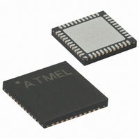
ATMEGA644P-A15MZ Atmel, ATMEGA644P-A15MZ Datasheet - Page 126

ATMEGA644P-A15MZ
Manufacturer Part Number
ATMEGA644P-A15MZ
Description
MCU AVR 64KB FLASH 16MHZ 44QFN
Manufacturer
Atmel
Series
AVR® ATmegar
Specifications of ATMEGA644P-A15MZ
Package / Case
44-VQFN Exposed Pad
Voltage - Supply (vcc/vdd)
2.7 V ~ 5.5 V
Operating Temperature
-40°C ~ 125°C
Speed
16MHz
Number Of I /o
32
Eeprom Size
2K x 8
Core Processor
AVR
Program Memory Type
FLASH
Ram Size
4K x 8
Program Memory Size
64KB (64K x 8)
Data Converters
A/D 8x10b
Oscillator Type
Internal
Peripherals
Brown-out Detect/Reset, POR, PWM, WDT
Connectivity
I²C, SPI, UART/USART
Core Size
8-Bit
Lead Free Status / RoHS Status
Lead free / RoHS Compliant
Available stocks
Company
Part Number
Manufacturer
Quantity
Price
Company:
Part Number:
ATMEGA644P-A15MZ
Manufacturer:
ATMEL
Quantity:
3 500
Part Number:
ATMEGA644P-A15MZ
Manufacturer:
ATMEL/爱特梅尔
Quantity:
20 000
- Current page: 126 of 377
- Download datasheet (7Mb)
126
ATmega164P/324P/644P
In inverting Output Compare mode, the operation is inverted. The dual-slope operation has
lower maximum operation frequency than single slope operation. However, due to the symmet-
ric feature of the dual-slope PWM modes, these modes are preferred for motor control
applications.
The PWM resolution for the phase correct PWM mode can be fixed to 8-, 9-, or 10-bit, or defined
by either ICRn or OCRnA. The minimum resolution allowed is 2-bit (ICRn or OCRnA set to
0x0003), and the maximum resolution is 16-bit (ICRn or OCRnA set to MAX). The PWM resolu-
tion in bits can be calculated by using the following equation:
In phase correct PWM mode the counter is incremented until the counter value matches either
one of the fixed values 0x00FF, 0x01FF, or 0x03FF (WGMn3:0 = 1, 2, or 3), the value in ICRn
(WGMn3:0 = 10), or the value in OCRnA (WGMn3:0 = 11). The counter has then reached the
TOP and changes the count direction. The TCNTn value will be equal to TOP for one timer clock
cycle. The timing diagram for the phase correct PWM mode is shown on
shows phase correct PWM mode when OCRnA or ICRn is used to define TOP. The TCNTn
value is in the timing diagram shown as a histogram for illustrating the dual-slope operation. The
diagram includes non-inverted and inverted PWM outputs. The small horizontal line marks on
the TCNTn slopes represent compare matches between OCRnx and TCNTn. The OCnx Inter-
rupt Flag will be set when a compare match occurs.
Figure 14-8. Phase Correct PWM Mode, Timing Diagram
The Timer/Counter Overflow Flag (TOVn) is set each time the counter reaches BOTTOM. When
either OCRnA or ICRn is used for defining the TOP value, the OCnA or ICFn Flag is set accord-
ingly at the same timer clock cycle as the OCRnx Registers are updated with the double buffer
value (at TOP). The Interrupt Flags can be used to generate an interrupt each time the counter
reaches the TOP or BOTTOM value.
TCNTn
OCnx
OCnx
Period
1
R
PCPWM
2
=
log
---------------------------------- -
log
TOP
3
2
+
1
4
Figure
OCRnx/TOP Update and
OCnA Interrupt Flag Set
or ICFn Interrupt Flag Set
(Interrupt on TOP)
TOVn Interrupt Flag Set
(Interrupt on Bottom)
14-8. The figure
(COMnx1:0 = 2)
(COMnx1:0 = 3)
7674F–AVR–09/09
Related parts for ATMEGA644P-A15MZ
Image
Part Number
Description
Manufacturer
Datasheet
Request
R

Part Number:
Description:
Manufacturer:
Atmel Corporation
Datasheet:

Part Number:
Description:
Manufacturer:
Atmel Corporation
Datasheet:

Part Number:
Description:
IC MCU AVR 64K FLASH 44-TQFP
Manufacturer:
Atmel
Datasheet:

Part Number:
Description:
IC MCU AVR 64K FLASH 44-QFN
Manufacturer:
Atmel
Datasheet:

Part Number:
Description:
MCU AVR 64K FLASH 20MHZ 44-TQFP
Manufacturer:
Atmel
Datasheet:

Part Number:
Description:
IC MCU AVR 64K FLASH 40-DIP
Manufacturer:
Atmel
Datasheet:

Part Number:
Description:
MCU AVR 64K FLASH 20MHZ 44TQFP
Manufacturer:
Atmel
Datasheet:

Part Number:
Description:
MCU AVR 64K FLASH 20MHZ 44QFN
Manufacturer:
Atmel
Datasheet:

Part Number:
Description:
MCU AVR 64K FLASH 20MHZ 44-QFN
Manufacturer:
Atmel
Datasheet:

Part Number:
Description:
MCU AVR 64K FLASH 20MHZ 40-PDIP
Manufacturer:
Atmel
Datasheet:

Part Number:
Description:
MCU AVR 64K FLASH 15MHZ 44-TQFP
Manufacturer:
Atmel
Datasheet:


