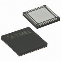
ATMEGA644P-A15MZ Atmel, ATMEGA644P-A15MZ Datasheet - Page 300

ATMEGA644P-A15MZ
Manufacturer Part Number
ATMEGA644P-A15MZ
Description
MCU AVR 64KB FLASH 16MHZ 44QFN
Manufacturer
Atmel
Series
AVR® ATmegar
Specifications of ATMEGA644P-A15MZ
Package / Case
44-VQFN Exposed Pad
Voltage - Supply (vcc/vdd)
2.7 V ~ 5.5 V
Operating Temperature
-40°C ~ 125°C
Speed
16MHz
Number Of I /o
32
Eeprom Size
2K x 8
Core Processor
AVR
Program Memory Type
FLASH
Ram Size
4K x 8
Program Memory Size
64KB (64K x 8)
Data Converters
A/D 8x10b
Oscillator Type
Internal
Peripherals
Brown-out Detect/Reset, POR, PWM, WDT
Connectivity
I²C, SPI, UART/USART
Core Size
8-Bit
Lead Free Status / RoHS Status
Lead free / RoHS Compliant
Available stocks
Company
Part Number
Manufacturer
Quantity
Price
Company:
Part Number:
ATMEGA644P-A15MZ
Manufacturer:
ATMEL
Quantity:
3 500
Part Number:
ATMEGA644P-A15MZ
Manufacturer:
ATMEL/爱特梅尔
Quantity:
20 000
- Current page: 300 of 377
- Download datasheet (7Mb)
25.6
25.6.1
300
Parallel Programming Parameters, Pin Mapping, and Commands
ATmega164P/324P/644P
Signal Names
This section describes how to parallel program and verify Flash Program memory, EEPROM
Data memory, Memory Lock bits, and Fuse bits in the ATmega164P/324P/644P. Pulses are
assumed to be at least 250 ns unless otherwise noted.
In this section, some pins of the ATmega164P/324P/644P are referenced by signal names
describing their functionality during parallel programming, see
ure 25-9 on page
The XA1/XA0 pins determine the action executed when the XTAL1 pin is given a positive pulse.
The bit coding is shown in
When pulsing WR or OE, the command loaded determines the action executed. The different
commands are shown in
Figure 25-1. Parallel Programming
Note:
Table 25-9.
Programming Mode
Signal Name in
RDY/BSY
1. Unused Pins should be left floating.
BS1
XA0
XA1
WR
OE
Pin Name Mapping
300. Pins not described in the following table are referenced by pin names.
Table 25-13 on page
RDY/BSY
Pin Name
Table 25-12 on page
PAGEL
+12 V
BS1
XA0
XA1
BS2
PD1
PD2
PD3
PD4
PD5
PD6
WR
OE
(1)
I/O
PD1
PD2
PD3
PD4
PD5
PD6
PD7
RESET
XTAL1
GND
O
PA0
I
I
I
I
I
Function
0: Device is busy programming, 1: Device is ready for
new command.
Output Enable (Active low).
Write Pulse (Active low).
Byte Select 1.
XTAL Action Bit 0
XTAL Action Bit 1
301.
301.
PB7 - PB0
AVCC
VCC
+5V
+5V
Figure 25-1 on page 300
DATA
7674F–AVR–09/09
and
Fig-
Related parts for ATMEGA644P-A15MZ
Image
Part Number
Description
Manufacturer
Datasheet
Request
R

Part Number:
Description:
Manufacturer:
Atmel Corporation
Datasheet:

Part Number:
Description:
Manufacturer:
Atmel Corporation
Datasheet:

Part Number:
Description:
IC MCU AVR 64K FLASH 44-TQFP
Manufacturer:
Atmel
Datasheet:

Part Number:
Description:
IC MCU AVR 64K FLASH 44-QFN
Manufacturer:
Atmel
Datasheet:

Part Number:
Description:
MCU AVR 64K FLASH 20MHZ 44-TQFP
Manufacturer:
Atmel
Datasheet:

Part Number:
Description:
IC MCU AVR 64K FLASH 40-DIP
Manufacturer:
Atmel
Datasheet:

Part Number:
Description:
MCU AVR 64K FLASH 20MHZ 44TQFP
Manufacturer:
Atmel
Datasheet:

Part Number:
Description:
MCU AVR 64K FLASH 20MHZ 44QFN
Manufacturer:
Atmel
Datasheet:

Part Number:
Description:
MCU AVR 64K FLASH 20MHZ 44-QFN
Manufacturer:
Atmel
Datasheet:

Part Number:
Description:
MCU AVR 64K FLASH 20MHZ 40-PDIP
Manufacturer:
Atmel
Datasheet:

Part Number:
Description:
MCU AVR 64K FLASH 15MHZ 44-TQFP
Manufacturer:
Atmel
Datasheet:


