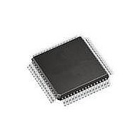
AT90CAN128-15AZ Atmel, AT90CAN128-15AZ Datasheet - Page 348

AT90CAN128-15AZ
Manufacturer Part Number
AT90CAN128-15AZ
Description
MCU AVR 128K FLASH 15MHZ 64TQFP
Manufacturer
Atmel
Series
AVR® 90CANr
Specifications of AT90CAN128-15AZ
Package / Case
64-TQFP, 64-VQFP
Voltage - Supply (vcc/vdd)
2.7 V ~ 5.5 V
Operating Temperature
-40°C ~ 125°C
Speed
16MHz
Number Of I /o
53
Eeprom Size
4K x 8
Core Processor
AVR
Program Memory Type
FLASH
Ram Size
4K x 8
Program Memory Size
128KB (128K x 8)
Data Converters
A/D 8x10b
Oscillator Type
Internal
Peripherals
Brown-out Detect/Reset, POR, PWM, WDT
Connectivity
CAN, I²C, SPI, UART/USART
Core Size
8-Bit
Processor Series
AT90CANx
Core
AVR8
Data Bus Width
8 bit
Data Ram Size
4 KB
Interface Type
CAN, SPI, UART
Maximum Clock Frequency
16 MHz
Number Of Programmable I/os
53
Number Of Timers
4
Maximum Operating Temperature
+ 125 C
Mounting Style
SMD/SMT
3rd Party Development Tools
EWAVR, EWAVR-BL
Development Tools By Supplier
ATAVRDRAGON, ATSTK500, ATSTK600, ATAVRISP2, ATDVK90CAN1, ATADAPCAN01
Minimum Operating Temperature
- 40 C
On-chip Adc
10 bit, 8 Channel
Cpu Family
90C
Device Core
AVR
Device Core Size
8b
Frequency (max)
16MHz
Total Internal Ram Size
4KB
# I/os (max)
53
Number Of Timers - General Purpose
4
Operating Supply Voltage (typ)
3.3/5V
Operating Supply Voltage (max)
5.5V
Operating Supply Voltage (min)
2.7V
Instruction Set Architecture
RISC
Operating Temp Range
-40C to 125C
Operating Temperature Classification
Automotive
Mounting
Surface Mount
Pin Count
64
Package Type
TQFP
Lead Free Status / RoHS Status
Lead free / RoHS Compliant
Available stocks
Company
Part Number
Manufacturer
Quantity
Price
Company:
Part Number:
AT90CAN128-15AZ
Manufacturer:
SAMSUNG
Quantity:
1 001
Company:
Part Number:
AT90CAN128-15AZ
Manufacturer:
ATMEL
Quantity:
1 000
Part Number:
AT90CAN128-15AZ
Manufacturer:
ATMEL/爱特梅尔
Quantity:
20 000
- Current page: 348 of 428
- Download datasheet (6Mb)
25.6.13
25.6.14
25.7
25.7.1
348
SPI Serial Programming Overview
AT90CAN32/64/128
Reading the Signature Bytes
Reading the Calibration Byte
Signal Names
Figure 25-6. Mapping Between BS1, BS2 and the Fuse and Lock Bits During Read
The algorithm for reading the Signature bytes is as follows (refer to
page 342
The algorithm for reading the Calibration byte is as follows (refer to
page 342
This section describes how to serial program and verify Flash Program memory, EEPROM Data
memory, Memory Lock bits, and Fuse bits in the AT90CAN32/64/128.
Both the Flash and EEPROM memory arrays can be programmed using the serial SPI bus while
RESET is pulled to GND. The serial interface consists of pins SCK, MOSI (input) and MISO (out-
put). After RESET is set low, the Programming Enable instruction needs to be executed first
before program/erase operations can be executed. NOTE, in
mapping for SPI programming is listed. Not all parts use the SPI pins dedicated for the internal
SPI interface. Note that throughout the description about Serial downloading, MOSI and MISO
are used to describe the serial data in and serial data out respectively. For AT90CAN32/64/128
these pins are mapped to PDI (PE0) and PDO (PE1).
1. A: Load Command “0000 1000”.
2. B: Load Address Low Byte (0x00 - 0x02).
3. Set OE to “0”, and BS1 to “0”. The selected Signature byte can now be read at DATA.
4. Set OE to “1”.
1. A: Load Command “0000 1000”.
2. B: Load Address Low Byte, 0x00.
3. Set OE to “0”, and BS1 to “1”. The Calibration byte can now be read at DATA.
4. Set OE to “1”.
for details on Command and Address loading):
for details on Command and Address loading):
Extended Fuse Byte
Fuse High Byte
Fuse Low Byte
Lock Bits
BS2
BS2
0
1
0
1
BS1
Table 25-13 on page
0
1
“Programming the Flash” on
“Programming the Flash” on
DATA
7679H–CAN–08/08
349, the pin
Related parts for AT90CAN128-15AZ
Image
Part Number
Description
Manufacturer
Datasheet
Request
R

Part Number:
Description:
DEV KIT FOR AVR/AVR32
Manufacturer:
Atmel
Datasheet:

Part Number:
Description:
INTERVAL AND WIPE/WASH WIPER CONTROL IC WITH DELAY
Manufacturer:
ATMEL Corporation
Datasheet:

Part Number:
Description:
Low-Voltage Voice-Switched IC for Hands-Free Operation
Manufacturer:
ATMEL Corporation
Datasheet:

Part Number:
Description:
MONOLITHIC INTEGRATED FEATUREPHONE CIRCUIT
Manufacturer:
ATMEL Corporation
Datasheet:

Part Number:
Description:
AM-FM Receiver IC U4255BM-M
Manufacturer:
ATMEL Corporation
Datasheet:

Part Number:
Description:
Monolithic Integrated Feature Phone Circuit
Manufacturer:
ATMEL Corporation
Datasheet:

Part Number:
Description:
Multistandard Video-IF and Quasi Parallel Sound Processing
Manufacturer:
ATMEL Corporation
Datasheet:

Part Number:
Description:
High-performance EE PLD
Manufacturer:
ATMEL Corporation
Datasheet:

Part Number:
Description:
8-bit Flash Microcontroller
Manufacturer:
ATMEL Corporation
Datasheet:

Part Number:
Description:
2-Wire Serial EEPROM
Manufacturer:
ATMEL Corporation
Datasheet:


