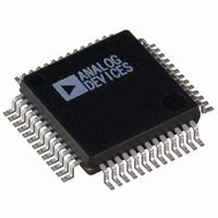
ADUC847BSZ62-3 Analog Devices Inc, ADUC847BSZ62-3 Datasheet - Page 44

ADUC847BSZ62-3
Manufacturer Part Number
ADUC847BSZ62-3
Description
IC MCU FLASH W/24BIT ADC 52MQFP
Manufacturer
Analog Devices Inc
Series
MicroConverter® ADuC8xxr
Datasheet
1.EVAL-ADUC845QSZ.pdf
(108 pages)
Specifications of ADUC847BSZ62-3
Core Size
8-Bit
Program Memory Size
62KB (62K x 8)
Oscillator Type
Internal
Core Processor
8052
Speed
12.58MHz
Connectivity
I²C, SPI, UART/USART
Peripherals
POR, PSM, PWM, Temp Sensor, WDT
Number Of I /o
34
Program Memory Type
FLASH
Eeprom Size
4K x 8
Ram Size
2.25K x 8
Voltage - Supply (vcc/vdd)
2.7 V ~ 3.6 V
Data Converters
A/D 10x24b; D/A 1x12b, 2x16b
Operating Temperature
-40°C ~ 125°C
Package / Case
52-MQFP, 52-PQFP
Controller Family/series
(8052) ADUC
No. Of I/o's
32
Ram Memory Size
2304Byte
Cpu Speed
12.58MHz
No. Of Timers
4
No. Of
RoHS Compliant
Package
52MQFP
Device Core
8052
Family Name
ADuC8xx
Maximum Speed
12.85 MHz
Operating Supply Voltage
3.3|5 V
Data Bus Width
8 Bit
Number Of Programmable I/os
24
Interface Type
I2C/SPI/UART
On-chip Adc
10-chx24-bit
On-chip Dac
1-chx12-bit
Number Of Timers
3
Lead Free Status / RoHS Status
Lead free / RoHS Compliant
For Use With
EVAL-ADUC847QSZ - KIT DEV QUICK START FOR ADUC847
Lead Free Status / RoHS Status
Lead free / RoHS Compliant
Available stocks
Company
Part Number
Manufacturer
Quantity
Price
Company:
Part Number:
ADUC847BSZ62-3
Manufacturer:
Analog Devices Inc
Quantity:
10 000
ADuC845/ADuC847/ADuC848
ADC0CON2 (PRIMARY ADC CHANNEL SELE
ADC0CON2 is used to select a reference source and channel for the primary ADC.
SFR Address:
Power-On Default:
Bit Addressable:
Table 26. ADC0CON2 SFR Bit Designations
Bit N
7, 6
5
4
3, 2, 1, 0
Note that because the reference-detect does not operate on the REFIN2± pair, the REFIN2± pins can go below 1 V.
o.
Name
XREF1, XREF0
–––
–––
CH3, CH2, CH1, CH0
E6H
00H
No
Descr
Primary ADC Exte
Set by the user to enable the primary ADC to use the external reference via REFIN± or REFIN2±.
Cleared by the user to enable the primary ADC to use the internal band gap reference (V
XREF1
0
0
1
1
Not Implemented. Write Don’t Care.
Not Implemented. Write Don’t Care.
Primary ADC Channel Select Bits. Written by the user to select the primary ADC channel as follows:
CH3
0
0
0
0
0
0
0
0
1
1
1
1
1
1
1
1
iption
CH2
0
0
0
0
1
1
1
1
0
0
0
0
1
1
1
1
XREF0
0
1
0
1
CH1
0
0
1
1
0
0
1
1
0
0
1
1
0
0
1
1
rna
Internal 1.25 V Reference.
REFIN± Selected.
REFIN2± (AIN3/AIN4) Selected.
Reserved.
CT REGISTER)
l Reference Sel
CH0
0
1
0
1
0
1
0
1
0
1
0
1
0
1
0
1
Rev. B | Page 44 of 108
Selected Primary ADC Input Channel.
AIN1–AINCOM
AIN2–AINCOM
AIN3–AINCOM
AIN4–AINCOM
AIN5–AINCOM
AIN6–AINCOM
AIN7–AINCOM
AIN8–AINCOM
AIN
pack
AIN10–AINCOM (LFCSP package only; not a valid selection on the MQFP
package)
AIN1–AIN2
AIN3–AIN4
AIN5–AIN6
AIN7–AIN8
AIN
package)
AINCOM–AINCOM
9–AINCOM (LFCSP package only; not a valid selection on the MQFP
9–AIN10 (LFCSP package only; not a valid selection on the MQFP
ect
age)
Bit.
REF
= 1.25 V).


