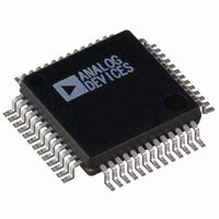
ADUC847BSZ62-3 Analog Devices Inc, ADUC847BSZ62-3 Datasheet - Page 61

ADUC847BSZ62-3
Manufacturer Part Number
ADUC847BSZ62-3
Description
IC MCU FLASH W/24BIT ADC 52MQFP
Manufacturer
Analog Devices Inc
Series
MicroConverter® ADuC8xxr
Datasheet
1.EVAL-ADUC845QSZ.pdf
(108 pages)
Specifications of ADUC847BSZ62-3
Core Size
8-Bit
Program Memory Size
62KB (62K x 8)
Oscillator Type
Internal
Core Processor
8052
Speed
12.58MHz
Connectivity
I²C, SPI, UART/USART
Peripherals
POR, PSM, PWM, Temp Sensor, WDT
Number Of I /o
34
Program Memory Type
FLASH
Eeprom Size
4K x 8
Ram Size
2.25K x 8
Voltage - Supply (vcc/vdd)
2.7 V ~ 3.6 V
Data Converters
A/D 10x24b; D/A 1x12b, 2x16b
Operating Temperature
-40°C ~ 125°C
Package / Case
52-MQFP, 52-PQFP
Controller Family/series
(8052) ADUC
No. Of I/o's
32
Ram Memory Size
2304Byte
Cpu Speed
12.58MHz
No. Of Timers
4
No. Of
RoHS Compliant
Package
52MQFP
Device Core
8052
Family Name
ADuC8xx
Maximum Speed
12.85 MHz
Operating Supply Voltage
3.3|5 V
Data Bus Width
8 Bit
Number Of Programmable I/os
24
Interface Type
I2C/SPI/UART
On-chip Adc
10-chx24-bit
On-chip Dac
1-chx12-bit
Number Of Timers
3
Lead Free Status / RoHS Status
Lead free / RoHS Compliant
For Use With
EVAL-ADUC847QSZ - KIT DEV QUICK START FOR ADUC847
Lead Free Status / RoHS Status
Lead free / RoHS Compliant
Available stocks
Company
Part Number
Manufacturer
Quantity
Price
Company:
Part Number:
ADUC847BSZ62-3
Manufacturer:
Analog Devices Inc
Quantity:
10 000
I
The ADuC845/ADuC847/ADuC848 support a fully licensed
I
hardware slave and software master. SDATA (Pin 27 on the
MQFP package and Pin 29 on the LFCSP package) is the data
I/O pin. SCLK (Pin 26 on the MQFP package and Pin 28 on the
LFCSP package) is the serial interface clock for the SPI interface.
The I
pin/function multiplexing. The I
the ADuC845/ADuC847/ADuC848 also includes a second
address register (I2CADD1) at SFR Address F2H with a default
power-on value of 7FH. The I
the user and is not multiplexed with any other I/O functionality
on the chip. This means that the I
used at the same time.
Table 40. I2CCON SFR Bit Designations
Bit No.
7
6
5
4
3
2
1
0
2
2
C serial interface. The I
C SERIAL INTERFACE
2
C interface on the parts is fully independent of all other
Name
MDO
MDE
MCO
MDI
I2CM
I2CRS
I2CTX
I2CI
Description
I
This data bit is used to implement a master I
the SDATA pin if the data output enable bit (MDE) is set.
I
Set by the user to enable the SDATA pin as an output (Tx).
Cleared by the user to enable the SDATA pin as an input (Rx).
I
This bit is used to implement the SCLK for a master I
the SCLK pin.
I
This data bit is used to implement a master I
this bit on an SCLK transition if the data output enable (MDE) bit is 0.
I
Set by the user to enable I
Cleared by the user to enable I
I
Set by the user to reset the I
Cleared by the user code for normal I
I
Set by the MicroConverter if the I
Cleared by the MicroConverter if the I
I
Set by the MicroConverter after a byte has been transmitted or received.
Cleared by the MicroConverter when the user code reads the I2CDAT SFR. I2CI should not be cleared by user code.
2
2
2
2
2
2
2
2
C Software Master Data Output Bit (master mode only).
C Software Output Enable Bit (master mode only).
C Software Master Clock Output Bit (master mode only).
C Software Master Data Input Bit (master mode only).
C Master/Slave Mode Bit.
C Reset Bit (slave mode only).
C Direction Transfer Bit (slave mode only).
C Interrupt Bit (slave mode only).
2
C interface is implemented as a full
2
C interface is always available to
2
C interface incorporated on
2
C and SPI interfaces can be
2
C software master mode.
2
C interface.
2
C hardware slave mode.
2
C interface is transmitting.
2
2
Rev. B | Page 61 of 108
C operation.
C interface is receiving.
2
2
C transmitter interface in software. Data written to this bit is output on
C receiver interface in software. Data on the SDATA pin is latched into
Note that when using the I
they both use the same interrupt routine (Vector Address 3BH).
When an interrupt occurs from one of these, it is necessary to
interrogate each interface to see which one has triggered the ISR
request.
The four SFRs that are used to control the I
described next.
I2CCON—I
SFR Address:
Power-On Default:
Bit Addressable:
2
C transmitter in software. Data written to this bit is output on
2
C Control Register
ADuC845/ADuC847/ADuC848
E8H
00H
Yes
2
C and SPI interfaces simultaneously,
2
C interface are


