MC56F8011VFAE Freescale Semiconductor, MC56F8011VFAE Datasheet - Page 111
MC56F8011VFAE
Manufacturer Part Number
MC56F8011VFAE
Description
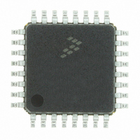
IC DIGITAL SIGNAL CTLR 32-LQFP
Manufacturer
Freescale Semiconductor
Series
56F8xxxr
Datasheet
1.MC56F8013VFAE.pdf
(126 pages)
Specifications of MC56F8011VFAE
Core Processor
56800
Core Size
16-Bit
Speed
32MHz
Connectivity
I²C, SCI, SPI
Peripherals
POR, PWM, WDT
Number Of I /o
26
Program Memory Size
12KB (6K x 16)
Program Memory Type
FLASH
Ram Size
1K x 16
Voltage - Supply (vcc/vdd)
3 V ~ 3.6 V
Data Converters
A/D 6x12b
Oscillator Type
Internal
Operating Temperature
-40°C ~ 105°C
Package / Case
32-LQFP
Product
DSCs
Data Bus Width
16 bit
Processor Series
MC56F80xx
Core
56800E
Numeric And Arithmetic Format
Fixed-Point
Device Million Instructions Per Second
32 MIPs
Maximum Clock Frequency
32 MHz
Number Of Programmable I/os
26
Data Ram Size
2 KB
Operating Supply Voltage
3.3 V
Maximum Operating Temperature
+ 105 C
Mounting Style
SMD/SMT
Development Tools By Supplier
MC56F8037EVM, DEMO56F8014-EE, DEMO56F8013-EE
Interface Type
SCI, SPI, I2C
Minimum Operating Temperature
- 40 C
For Use With
CPA56F8013 - BOARD SOCKET FOR MC56F8013APMOTOR56F8000E - KIT DEMO MOTOR CTRL SYSTEM
Lead Free Status / RoHS Status
Lead free / RoHS Compliant
Eeprom Size
-
Lead Free Status / Rohs Status
Lead free / RoHS Compliant
Available stocks
Company
Part Number
Manufacturer
Quantity
Price
Company:

Part Number:
MC56F8011VFAE
Manufacturer:
Freescale
Quantity:
1
Company:
Part Number:
MC56F8011VFAE
Manufacturer:
Freescale Semiconductor
Quantity:
10 000


10.12 Inter-Integrated Circuit Interface (I
Freescale Semiconductor
1. A device must internally provide a hold time of at least 300ns for the SDA signal (referred to the V
2. The maximum t
3. A Fast mode I
4. C
SCL Clock Frequency
Hold time (repeated )
START condition. After
this period, the first clock
pulse is generated.
LOW period of the SCL
clock
HIGH period of the SCL
clock
Set-up time for a repeated
START condition
Data hold time for I
devices
Data set-up time
Rise time of both SDA and
SCL signals
Fall time of both SDA and
SCL signals
Set-up time for STOP
condition
Bus free time between
STOP and START
condition
Pulse width of spikes that
must be suppressed by
the input filter
signal) to bridge the undefined region of the falling edge of SCL.
must then be met. This will automatically be the case if the device does not stretch the LOW period of the SCL signal.
If such a device does stretch the LOW period of the SCL signal, it must output the next data bit to the SDA line
t
released.
rmax
b
= total capacitance of the one bus line in pF.
Characteristic
+ t
SU; DAT
2
C bus device can be used in a Standard mode I
HD; DAT
= 1000 + 250 = 1250ns (according to the Standard mode I
2
C bus
has only to be met if the device does not stretch the LOW period (t
Symbol
t
t
t
t
t
HD; STA
HD; DAT
SU; DAT
SU; STO
SU; STA
t
t
f
t
HIGH
LOW
BUF
t
SCL
SP
t
t
r
f
56F8013/56F8011 Data Sheet, Rev. 12
Table 10-17 I
Minimum
250
N/A
4.0
4.7
4.0
4.7
4.0
4.7
0
Standard Mode
0
1
Maximum
2
2
C Timing
3.45
C bus system, but the requirement t
1000
100
300
N/A
2
2
2
C bus specification) before the SCL line is
C) Timing
2 +0.1C
2 +0.1C
Minimum
100
1.25
0.6
0.6
0.6
0.6
1.3
0.0
0
0
1
3
Inter-Integrated Circuit Interface (I2C) Timing
Fast Mode
b
b
4
4
LOW
Maximum
) of the SCL signal.
0.9
400
300
300
50
2
IH
SU; DAT
min of the SCL
> = 250ns
Unit
kHz
μs
μs
μs
μs
μs
ns
ns
ns
μs
μs
ns
111
Related parts for MC56F8011VFAE
Image
Part Number
Description
Manufacturer
Datasheet
Request
R

Part Number:
Description:
16-bit Digital Signal Controllers
Manufacturer:
Freescale Semiconductor, Inc
Datasheet:
Part Number:
Description:
Manufacturer:
Freescale Semiconductor, Inc
Datasheet:
Part Number:
Description:
Manufacturer:
Freescale Semiconductor, Inc
Datasheet:
Part Number:
Description:
Manufacturer:
Freescale Semiconductor, Inc
Datasheet:
Part Number:
Description:
Manufacturer:
Freescale Semiconductor, Inc
Datasheet:
Part Number:
Description:
Manufacturer:
Freescale Semiconductor, Inc
Datasheet:
Part Number:
Description:
Manufacturer:
Freescale Semiconductor, Inc
Datasheet:
Part Number:
Description:
Manufacturer:
Freescale Semiconductor, Inc
Datasheet:
Part Number:
Description:
Manufacturer:
Freescale Semiconductor, Inc
Datasheet:
Part Number:
Description:
Manufacturer:
Freescale Semiconductor, Inc
Datasheet:
Part Number:
Description:
Manufacturer:
Freescale Semiconductor, Inc
Datasheet:
Part Number:
Description:
Manufacturer:
Freescale Semiconductor, Inc
Datasheet:
Part Number:
Description:
Manufacturer:
Freescale Semiconductor, Inc
Datasheet:
Part Number:
Description:
Manufacturer:
Freescale Semiconductor, Inc
Datasheet:
Part Number:
Description:
Manufacturer:
Freescale Semiconductor, Inc
Datasheet: