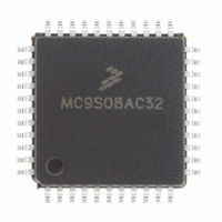
MC9S08AC32CFUE Freescale Semiconductor, MC9S08AC32CFUE Datasheet - Page 273

MC9S08AC32CFUE
Manufacturer Part Number
MC9S08AC32CFUE
Description
IC MCU 8BIT 32K FLASH 64-QFP
Manufacturer
Freescale Semiconductor
Series
HCS08r
Specifications of MC9S08AC32CFUE
Core Processor
HCS08
Core Size
8-Bit
Speed
40MHz
Connectivity
I²C, SCI, SPI
Peripherals
LVD, POR, PWM, WDT
Number Of I /o
54
Program Memory Size
32KB (32K x 8)
Program Memory Type
FLASH
Ram Size
2K x 8
Voltage - Supply (vcc/vdd)
2.7 V ~ 5.5 V
Data Converters
A/D 16x10b
Oscillator Type
Internal
Operating Temperature
-40°C ~ 85°C
Package / Case
64-QFP
Processor Series
S08AC
Core
HCS08
Data Bus Width
8 bit
Data Ram Size
2 KB
Interface Type
I2C, SCI, SPI
Maximum Clock Frequency
20 MHz
Number Of Programmable I/os
54
Number Of Timers
3
Maximum Operating Temperature
+ 85 C
Mounting Style
SMD/SMT
3rd Party Development Tools
EWS08
Development Tools By Supplier
DEMO9S08AC60E, DEMOACEX, DEMOACKIT, DCF51AC256, DC9S08AC128, DC9S08AC16, DC9S08AC60, DEMO51AC256KIT
Minimum Operating Temperature
- 40 C
On-chip Adc
10 bit, 16 Channel
Cpu Family
HCS08
Device Core Size
8b
Frequency (max)
20MHz
Total Internal Ram Size
2KB
# I/os (max)
54
Number Of Timers - General Purpose
3
Operating Supply Voltage (typ)
3.3/5V
Operating Supply Voltage (max)
5.5V
Operating Supply Voltage (min)
2.7V
Instruction Set Architecture
CISC
Operating Temp Range
-40C to 85C
Operating Temperature Classification
Industrial
Mounting
Surface Mount
Pin Count
64
Package Type
PQFP
Lead Free Status / RoHS Status
Lead free / RoHS Compliant
Eeprom Size
-
Lead Free Status / Rohs Status
Lead free / RoHS Compliant
Available stocks
Company
Part Number
Manufacturer
Quantity
Price
Company:
Part Number:
MC9S08AC32CFUE
Manufacturer:
Freescale Semiconductor
Quantity:
10 000
Part Number:
MC9S08AC32CFUE
Manufacturer:
FREESCALE
Quantity:
20 000
- Current page: 273 of 348
- Download datasheet (4Mb)
In output compare mode, values are transferred to the corresponding timer channel registers only after both
8-bit halves of a 16-bit register have been written and according to the value of CLKSB:CLKSA bits, so:
The coherency sequence can be manually reset by writing to the channel status/control register
(TPMxCnSC).
An output compare event sets a flag bit (CHnF) which may optionally generate a CPU-interrupt request.
15.6.2.3
This type of PWM output uses the normal up-counting mode of the timer counter (CPWMS=0) and can
be used when other channels in the same TPM are configured for input capture or output compare
functions. The period of this PWM signal is determined by the value of the modulus register
(TPMxMODH:TPMxMODL) plus 1. The duty cycle is determined by the setting in the timer channel
register (TPMxCnVH:TPMxCnVL). The polarity of this PWM signal is determined by the setting in the
ELSnA control bit. 0% and 100% duty cycle cases are possible.
The output compare value in the TPM channel registers determines the pulse width (duty cycle) of the
PWM signal
width. If ELSnA=0, the counter overflow forces the PWM signal high, and the output compare forces the
PWM signal low. If ELSnA=1, the counter overflow forces the PWM signal low, and the output compare
forces the PWM signal high.
When the channel value register is set to 0x0000, the duty cycle is 0%. 100% duty cycle can be achieved
by setting the timer-channel register (TPMxCnVH:TPMxCnVL) to a value greater than the modulus
setting. This implies that the modulus setting must be less than 0xFFFF in order to get 100% duty cycle.
Because the TPM may be used in an 8-bit MCU, the settings in the timer channel registers are buffered to
ensure coherent 16-bit updates and to avoid unexpected PWM pulse widths. Writes to any of the registers
TPMxCnVH and TPMxCnVL, actually write to buffer registers. In edge-aligned PWM mode, values are
transferred to the corresponding timer-channel registers according to the value of CLKSB:CLKSA bits, so:
Freescale Semiconductor
•
•
•
•
If (CLKSB:CLKSA = 0:0), the registers are updated when the second byte is written
If (CLKSB:CLKSA not = 0:0), the registers are updated at the next change of the TPM counter
(end of the prescaler counting) after the second byte is written.
If (CLKSB:CLKSA = 0:0), the registers are updated when the second byte is written
If (CLKSB:CLKSA not = 0:0), the registers are updated after the both bytes were written, and the
TPM counter changes from (TPMxMODH:TPMxMODL - 1) to (TPMxMODH:TPMxMODL). If
(Figure
TPMxCHn
Edge-Aligned PWM Mode
OVERFLOW
15-15). The time between the modulus overflow and the output compare is the pulse
Figure 15-15. PWM Period and Pulse Width (ELSnA=0)
PULSE
WIDTH
PERIOD
MC9S08AC60 Series Data Sheet, Rev. 2
COMPARE
OUTPUT
OVERFLOW
COMPARE
OUTPUT
OVERFLOW
Chapter 15 Timer/PWM Module (S08TPMV3)
COMPARE
OUTPUT
273
Related parts for MC9S08AC32CFUE
Image
Part Number
Description
Manufacturer
Datasheet
Request
R
Part Number:
Description:
Manufacturer:
Freescale Semiconductor, Inc
Datasheet:
Part Number:
Description:
Manufacturer:
Freescale Semiconductor, Inc
Datasheet:
Part Number:
Description:
Manufacturer:
Freescale Semiconductor, Inc
Datasheet:
Part Number:
Description:
Manufacturer:
Freescale Semiconductor, Inc
Datasheet:
Part Number:
Description:
Manufacturer:
Freescale Semiconductor, Inc
Datasheet:
Part Number:
Description:
Manufacturer:
Freescale Semiconductor, Inc
Datasheet:
Part Number:
Description:
Manufacturer:
Freescale Semiconductor, Inc
Datasheet:
Part Number:
Description:
Manufacturer:
Freescale Semiconductor, Inc
Datasheet:
Part Number:
Description:
Manufacturer:
Freescale Semiconductor, Inc
Datasheet:
Part Number:
Description:
Manufacturer:
Freescale Semiconductor, Inc
Datasheet:
Part Number:
Description:
Manufacturer:
Freescale Semiconductor, Inc
Datasheet:
Part Number:
Description:
Manufacturer:
Freescale Semiconductor, Inc
Datasheet:
Part Number:
Description:
Manufacturer:
Freescale Semiconductor, Inc
Datasheet:
Part Number:
Description:
Manufacturer:
Freescale Semiconductor, Inc
Datasheet:
Part Number:
Description:
Manufacturer:
Freescale Semiconductor, Inc
Datasheet:


