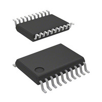
R5F21294SNSP#U0 Renesas Electronics America, R5F21294SNSP#U0 Datasheet - Page 227

R5F21294SNSP#U0
Manufacturer Part Number
R5F21294SNSP#U0
Description
MCU 3/5V 16K+2K 20PIN-SSOP
Manufacturer
Renesas Electronics America
Series
M16C™ M16C/R8C/Tiny/29r
Datasheet
1.R5F21282SNSPU0.pdf
(473 pages)
Specifications of R5F21294SNSP#U0
Core Processor
R8C
Core Size
16-Bit
Speed
20MHz
Connectivity
I²C, LIN, SIO, SSU, UART/USART
Peripherals
LED, POR, Voltage Detect, WDT
Number Of I /o
13
Program Memory Size
16KB (16K x 8)
Program Memory Type
FLASH
Ram Size
1K x 8
Voltage - Supply (vcc/vdd)
2.2 V ~ 5.5 V
Data Converters
A/D 4x10b
Oscillator Type
Internal
Operating Temperature
-20°C ~ 85°C
Package / Case
20-SSOP
Lead Free Status / RoHS Status
Lead free / RoHS Compliant
Eeprom Size
-
Available stocks
Company
Part Number
Manufacturer
Quantity
Price
- Current page: 227 of 473
- Download datasheet (5Mb)
R8C/28 Group, R8C/29 Group
Rev.2.10
REJ09B0279-0210
Table 14.22
j = A, B, or C
Count source
Count operation
PWM waveform
Count start conditions
Count stop conditions
Interrupt request
generation timing
TRCIOA/TRCTRG pin
function
TRCIOB pin function
TRCIOC and TRCIOD
pin functions
INT0 pin function
Read from timer
Write to timer
Select functions
Sep 26, 2008
Item
Specifications of PWM2 Mode
Page 208 of 441
f1, f2, f4, f8, f32, fOCO40M, or external signal (rising edge) input to TRCCLK pin
Increment TRC register
PWM period: 1/fk × (m + 1) (no TRCTRG input)
Active level width: 1/fk × (n - p)
Wait time from count start or trigger: 1/fk × (p + 1)
• Bits TCEG1 to TCEG0 in the TRCCR2 register are set to 00b (TRCTRG trigger
• Bits TCEG1 to TCEG0 in the TRCCR2 register are set to 01b, 10b, or 11b
• 0 (count stops) is written to the TSTART bit in the TRCMR register while the CSEL
• The count stops due to a compare match with TRCGRA while the CSEL bit in the
• Compare match (contents of TRC and TRCGRj registers match)
• The TRC register overflows
Programmable I/O port or TRCTRG input
PWM output
Programmable I/O port
Programmable I/O port, pulse output forced cutoff signal input, or INT0 interrupt
input
The count value can be read by reading the TRC register.
The TRC register can be written to.
• External trigger and valid edge selected
• Buffer operation (Refer to 14.3.3.2 Buffer Operation.)
• Pulse output forced cutoff signal input (Refer to 14.3.3.4 Forced Cutoff of Pulse
• Digital filter (Refer to 14.3.3.3 Digital Filter.)
disabled) or the CSEL bit in the TRCCR2 register is set to 0 (count continues).
(TRCTRG trigger enabled) and the TSTART bit in the TRCMR register is set to 1
(count starts).
bit in the TRCCR2 register is set to 0 or 1.
TRCCR2 register is set to 1
Output.)
fk: Count source frequency
m: TRCGRA register setting value
n: TRCGRB register setting value
p: TRCGRC register setting value
1 (count starts) is written to the TSTART bit in the TRCMR register.
A trigger is input to the TRCTRG pin
The TRCIOB pin outputs the initial level in accordance with the value of the TOB
bit in the TRCCR1 register. The TRC register retains the value before count stops.
The TRCIOB pin outputs the initial level. The TRC register retains the value before
count stops if the CCLR bit in the TRCCR1 register is set to 0. The TRC register is
set to 0000h if the CCLR bit in the TRCCR1 register is set to 1.
The edge or edges of the signal input to the TRCTRG pin can be used as the
PWM output trigger: rising edge, falling edge, or both rising and falling edges
TRCIOB output
TRCTRG input
m+1
n+1
p+1
n-p
Specification
(TRCTRG: Rising edge, active level is “H”)
n+1
p+1
n-p
14. Timers
Related parts for R5F21294SNSP#U0
Image
Part Number
Description
Manufacturer
Datasheet
Request
R

Part Number:
Description:
KIT STARTER FOR M16C/29
Manufacturer:
Renesas Electronics America
Datasheet:

Part Number:
Description:
KIT STARTER FOR R8C/2D
Manufacturer:
Renesas Electronics America
Datasheet:

Part Number:
Description:
R0K33062P STARTER KIT
Manufacturer:
Renesas Electronics America
Datasheet:

Part Number:
Description:
KIT STARTER FOR R8C/23 E8A
Manufacturer:
Renesas Electronics America
Datasheet:

Part Number:
Description:
KIT STARTER FOR R8C/25
Manufacturer:
Renesas Electronics America
Datasheet:

Part Number:
Description:
KIT STARTER H8S2456 SHARPE DSPLY
Manufacturer:
Renesas Electronics America
Datasheet:

Part Number:
Description:
KIT STARTER FOR R8C38C
Manufacturer:
Renesas Electronics America
Datasheet:

Part Number:
Description:
KIT STARTER FOR R8C35C
Manufacturer:
Renesas Electronics America
Datasheet:

Part Number:
Description:
KIT STARTER FOR R8CL3AC+LCD APPS
Manufacturer:
Renesas Electronics America
Datasheet:

Part Number:
Description:
KIT STARTER FOR RX610
Manufacturer:
Renesas Electronics America
Datasheet:

Part Number:
Description:
KIT STARTER FOR R32C/118
Manufacturer:
Renesas Electronics America
Datasheet:

Part Number:
Description:
KIT DEV RSK-R8C/26-29
Manufacturer:
Renesas Electronics America
Datasheet:

Part Number:
Description:
KIT STARTER FOR SH7124
Manufacturer:
Renesas Electronics America
Datasheet:

Part Number:
Description:
KIT STARTER FOR H8SX/1622
Manufacturer:
Renesas Electronics America
Datasheet:

Part Number:
Description:
KIT DEV FOR SH7203
Manufacturer:
Renesas Electronics America
Datasheet:


