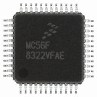
MC56F8322VFAE Freescale Semiconductor, MC56F8322VFAE Datasheet - Page 87

MC56F8322VFAE
Manufacturer Part Number
MC56F8322VFAE
Description
IC DSP 16BIT 60MHZ 48-LQFP
Manufacturer
Freescale Semiconductor
Series
56F8xxxr
Datasheet
1.MC56F8122VFAE.pdf
(136 pages)
Specifications of MC56F8322VFAE
Core Processor
56800
Core Size
16-Bit
Speed
60MHz
Connectivity
CAN, SCI, SPI
Peripherals
POR, PWM, Temp Sensor, WDT
Number Of I /o
21
Program Memory Size
40KB (20K x 16)
Program Memory Type
FLASH
Ram Size
6K x 16
Voltage - Supply (vcc/vdd)
2.25 V ~ 3.6 V
Data Converters
A/D 6x12b
Oscillator Type
Internal
Operating Temperature
-40°C ~ 105°C
Package / Case
48-LQFP
Data Bus Width
16 bit
Processor Series
MC56F83xx
Core
56800E
Numeric And Arithmetic Format
Fixed-Point
Device Million Instructions Per Second
40 MIPs
Maximum Clock Frequency
60 MHz
Number Of Programmable I/os
21
Data Ram Size
4 KB
Operating Supply Voltage
3.3 V
Maximum Operating Temperature
+ 105 C
Mounting Style
SMD/SMT
Interface Type
SCI, SPI, CAN
Minimum Operating Temperature
- 40 C
For Use With
MC56F8323EVME - BOARD EVALUATION MC56F8323
Lead Free Status / RoHS Status
Lead free / RoHS Compliant
Eeprom Size
-
Lead Free Status / Rohs Status
Lead free / RoHS Compliant
Available stocks
Company
Part Number
Manufacturer
Quantity
Price
Company:
Part Number:
MC56F8322VFAE
Manufacturer:
Freescale Semiconductor
Quantity:
10 000
Part Number:
MC56F8322VFAE
Manufacturer:
FREESCALE
Quantity:
20 000
Company:
Part Number:
MC56F8322VFAER2
Manufacturer:
Freescale Semiconductor
Quantity:
10 000
6.5.7.4
6.5.7.5
6.5.7.6
6.5.7.7
Selects clock to be muxed out on the CLKO pin.
6.5.8
All of the peripheral pins on the 56F8322 and 56F8122 share their I/O with GPIO ports. To select
peripheral or GPIO control, program the GPIOx_PER register. When SPI 0 and SCI 1, Quad Timer C and
SCI 0, or PWMA and SPI 1 are multiplexed, there are two possible peripherals as well as the GPIO
functionality available for control of the I/O. The SIM_GPS register is used to determine which peripheral
has control. The default peripherals are SPI 0, Quad Timer C, and PWMA.
Note: PWM is NOT available in the 56F8122 device.
Freescale Semiconductor
Preliminary
•
•
•
•
•
•
•
•
•
•
•
•
•
•
•
•
•
•
•
•
•
•
•
0 = Peripheral output function of GPIOB[5] is defined to be INDEX0
1 = Peripheral output function of GPIOB[5] is defined to be SYS_CLK
0 = Peripheral output function of GPIOB[4] is defined to be HOME0
1 = Peripheral output function of GPIOB[4] is defined to be the prescaler clock (FREF, see
0 = CLKOUT output is enabled and will output the signal indicated by CLKOSEL
1 = CLKOUT is tri-stated
00000 = SYS_CLK (from ROCS - DEFAULT)
00001 = Reserved for factory test—56800E clock
00010 = Reserved for factory test—XRAM clock
00011 = Reserved for factory test—PFLASH odd clock
00100 = Reserved for factory test—PFLASH even clock
00101 = Reserved for factory test—BFLASH clock
00110 = Reserved for factory test—DFLASH clock
00111 = MSTR_OSC Oscillator output
01000 = F
01001 = Reserved for factory test—IPB clock
01010 = Reserved for factory test—Feedback (from OCCS, this is path to PLL)
01011 = Reserved for factory test—Prescaler clock (from OCCS)
01100 = Reserved for factory test—Postscaler clock (from OCCS)
01101 = Reserved for factory test—SYS_CLK2 (from OCCS)
01110 = Reserved for factory test—SYS_CLK_DIV2
01111 = Reserved for factory test—SYS_CLK_D
10000 = ADCA clock
SIM GPIO Peripheral Select Register (SIM_GPS)
INDEX0 (INDEX)—Bit 7
HOME0 (HOME)—Bit 6
Clockout Disable (CLKDIS)—Bit 5
CLockout Select (CLKOSEL)—Bits 4–0
out
(from OCCS)
56F8322 Technical Data, Rev. 16
Register Descriptions
Figure
3-4)
87


