MC9S12XDT256MAG Freescale Semiconductor, MC9S12XDT256MAG Datasheet - Page 692
MC9S12XDT256MAG
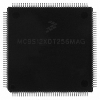
Manufacturer Part Number
MC9S12XDT256MAG
Description
IC MCU 256K FLASH 144-LQFP
Manufacturer
Freescale Semiconductor
Series
HCS12r
Datasheet
1.MC9S12XD64CAA.pdf
(1348 pages)
Specifications of MC9S12XDT256MAG
Core Processor
HCS12X
Core Size
16-Bit
Speed
80MHz
Connectivity
CAN, EBI/EMI, I²C, IrDA, LIN, SCI, SPI
Peripherals
LVD, POR, PWM, WDT
Number Of I /o
119
Program Memory Size
256KB (256K x 8)
Program Memory Type
FLASH
Eeprom Size
4K x 8
Ram Size
16K x 8
Voltage - Supply (vcc/vdd)
2.35 V ~ 5.5 V
Data Converters
A/D 24x10b
Oscillator Type
External
Operating Temperature
-40°C ~ 125°C
Package / Case
144-LQFP
Processor Series
S12XD
Core
HCS12
Data Bus Width
16 bit
Data Ram Size
16 KB
Interface Type
CAN/I2C/SCI/SPI
Maximum Clock Frequency
40 MHz
Number Of Programmable I/os
119
Number Of Timers
12
Operating Supply Voltage
0 V to 5.5 V
Maximum Operating Temperature
+ 125 C
Mounting Style
SMD/SMT
3rd Party Development Tools
EWHCS12
Development Tools By Supplier
EVB9S12XDP512E
Minimum Operating Temperature
- 40 C
On-chip Adc
2 (24-ch x 10-bit)
Lead Free Status / RoHS Status
Lead free / RoHS Compliant
Available stocks
Company
Part Number
Manufacturer
Quantity
Price

Company:
Part Number:
MC9S12XDT256MAG
Manufacturer:
Freescale Semiconductor
Quantity:
10 000


Chapter 19 S12X Debug (S12XDBGV2) Module
19.1.2
19.1.3
The DBG module can be used in all MCU functional modes.
During BDM hardware accesses and when the BDM module is active, CPU monitoring is disabled. Thus
breakpoints, comparators and bus tracing mapped to the CPU are disabled but accessing the DBG registers,
including comparator registers, is still possible. While in active BDM or during hardware BDM accesses,
694
•
•
•
•
•
•
•
Four comparators (A, B, C, and D):
— Comparators A and C compare the full address and the full 16-bit data bus
— Comparators A and C feature a data bus mask register
— Comparators B and D compare the full address bus only
— Each comparator can be configured to monitor either CPU or XGATE busses
— Each comparator features control of R/W and byte/word access cycles
— Comparisons can be used as triggers for the state sequencer
Three comparator modes:
— Simple address/data comparator match mode
— Inside address range mode, Addmin Address Addmax
— Outside address range match mode, Address Addmin or Address Addmax
Two types of triggers:
— Tagged: triggers just before a specific instruction begins execution
— Force: triggers on the first instruction boundary after a match occurs.
Three types of breakpoints:
— CPU breakpoint entering BDM on breakpoint (BDM)
— CPU breakpoint executing SWI on breakpoint (SWI)
— XGATE breakpoint
Three trigger modes independent of comparators:
— External instruction tagging (associated with CPU instructions only)
— XGATE S/W breakpoint request
— TRIG bit immediate software trigger
Three trace modes:
— Normal: change of flow (COF) bus information is stored (see
— Loop1: same as normal but inhibits consecutive duplicate source address entries
— Detail: address and data for all cycles except free cycles and opcode fetches are stored
4-stage state sequencer for trace buffer control:
— Tracing session trigger linked to final state of state sequencer
— Begin, end, and mid alignment of tracing to trigger
Mode”) for change of flow definition.
Features
Modes of Operation
MC9S12XDP512 Data Sheet, Rev. 2.21
Section 19.4.5.2.1, “Normal
Freescale Semiconductor
Related parts for MC9S12XDT256MAG
Image
Part Number
Description
Manufacturer
Datasheet
Request
R

Part Number:
Description:
16-BIT MICROPROCESSOR FAMILY
Manufacturer:
FREESCALE [Freescale Semiconductor, Inc]
Datasheet:

Part Number:
Description:
Manufacturer:
Freescale Semiconductor, Inc
Datasheet:
Part Number:
Description:
Manufacturer:
Freescale Semiconductor, Inc
Datasheet:
Part Number:
Description:
Manufacturer:
Freescale Semiconductor, Inc
Datasheet:
Part Number:
Description:
Manufacturer:
Freescale Semiconductor, Inc
Datasheet:
Part Number:
Description:
Manufacturer:
Freescale Semiconductor, Inc
Datasheet:
Part Number:
Description:
Manufacturer:
Freescale Semiconductor, Inc
Datasheet:
Part Number:
Description:
Manufacturer:
Freescale Semiconductor, Inc
Datasheet:
Part Number:
Description:
Manufacturer:
Freescale Semiconductor, Inc
Datasheet:
Part Number:
Description:
Manufacturer:
Freescale Semiconductor, Inc
Datasheet:
Part Number:
Description:
Manufacturer:
Freescale Semiconductor, Inc
Datasheet:
Part Number:
Description:
Manufacturer:
Freescale Semiconductor, Inc
Datasheet:
Part Number:
Description:
Manufacturer:
Freescale Semiconductor, Inc
Datasheet:
Part Number:
Description:
Manufacturer:
Freescale Semiconductor, Inc
Datasheet:
Part Number:
Description:
Manufacturer:
Freescale Semiconductor, Inc
Datasheet: