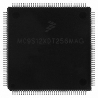
MC9S12XDT256MAG Freescale Semiconductor, MC9S12XDT256MAG Datasheet - Page 965

MC9S12XDT256MAG
Manufacturer Part Number
MC9S12XDT256MAG
Description
IC MCU 256K FLASH 144-LQFP
Manufacturer
Freescale Semiconductor
Series
HCS12r
Datasheet
1.MC9S12XD64CAA.pdf
(1348 pages)
Specifications of MC9S12XDT256MAG
Core Processor
HCS12X
Core Size
16-Bit
Speed
80MHz
Connectivity
CAN, EBI/EMI, I²C, IrDA, LIN, SCI, SPI
Peripherals
LVD, POR, PWM, WDT
Number Of I /o
119
Program Memory Size
256KB (256K x 8)
Program Memory Type
FLASH
Eeprom Size
4K x 8
Ram Size
16K x 8
Voltage - Supply (vcc/vdd)
2.35 V ~ 5.5 V
Data Converters
A/D 24x10b
Oscillator Type
External
Operating Temperature
-40°C ~ 125°C
Package / Case
144-LQFP
Processor Series
S12XD
Core
HCS12
Data Bus Width
16 bit
Data Ram Size
16 KB
Interface Type
CAN/I2C/SCI/SPI
Maximum Clock Frequency
40 MHz
Number Of Programmable I/os
119
Number Of Timers
12
Operating Supply Voltage
0 V to 5.5 V
Maximum Operating Temperature
+ 125 C
Mounting Style
SMD/SMT
3rd Party Development Tools
EWHCS12
Development Tools By Supplier
EVB9S12XDP512E
Minimum Operating Temperature
- 40 C
On-chip Adc
2 (24-ch x 10-bit)
Lead Free Status / RoHS Status
Lead free / RoHS Compliant
Available stocks
Company
Part Number
Manufacturer
Quantity
Price
Company:
Part Number:
MC9S12XDT256MAG
Manufacturer:
Freescale Semiconductor
Quantity:
10 000
- Current page: 965 of 1348
- Download datasheet (8Mb)
23.0.7.8
This port is associated with the CAN40 and SPI0. Port M pins PM[7:0] can be used for either
general purpose I/O, or with the CAN, SCI and SPI subsystems.
The CAN0, CAN4 and SPI0 pins can be re-routed. Refer to
Register
23.0.7.9
This port is associated with the PWM, SPI1 and SPI2. Port P pins PP[7:0] can be used for either
general purpose I/O, or with the PWM and SPI subsystems.
The pins are shared between the PWM channels and the SPI1 and SPI2. If the PWM is enabled the
pins become PWM output channels with the exception of pin 7 which can be PWM input or output.
If SPI1 or SPI2 are enabled and PWM is disabled, the respective pin configuration is determined
by status bits in the SPI.
The SPI1 and SPI2 pins can be re-routed. Refer to
(MODRR)”.
Port P offers 8 I/O pins with edge triggered interrupt capability in wired-OR fashion
(Section 23.0.8, “Pin
23.0.7.10 Port H
This port is associated with the SPI1, SPI2, SCI4. Port H pins PH[7:0] can be used for either
general purpose I/O, or with the SPI and SCI subsystems. Port H pins can be used with the routed
SPI1 and SPI2. Refer to
Port H offers 8 I/O pins with edge triggered interrupt capability
23.0.7.11 Port J
This port is associated with the chip selects CS0, CS1, CS2 and CS3 as well as with CAN4, CAN0,
IIC1, IIC0, and SCI2. Port J pins PJ[7:4] and PJ[2:0] can be used for either general purpose I/O, or
with the CAN, IIC, or SCI subsystems. If IIC takes precedence the associated pins become IIC
(MODRR)”.
Port M
Port P
PS[7:4] are not available in 80-pin packages.
PM[7:6] are not available in 80-pin packages.
PP[6] is not available in 80-pin packages.
Port H is not available in 80-pin packages.
Interrupts”).
Section 23.0.5.37, “Module Routing Register
NOTE
NOTE
NOTE
NOTE
Section 23.0.5.37, “Module Routing Register
Section 23.0.5.37, “Module Routing
(Section 23.0.8, “Pin
(MODRR)”.
Interrupts”).
Related parts for MC9S12XDT256MAG
Image
Part Number
Description
Manufacturer
Datasheet
Request
R

Part Number:
Description:
16-BIT MICROPROCESSOR FAMILY
Manufacturer:
FREESCALE [Freescale Semiconductor, Inc]
Datasheet:
Part Number:
Description:
Manufacturer:
Freescale Semiconductor, Inc
Datasheet:
Part Number:
Description:
Manufacturer:
Freescale Semiconductor, Inc
Datasheet:
Part Number:
Description:
Manufacturer:
Freescale Semiconductor, Inc
Datasheet:
Part Number:
Description:
Manufacturer:
Freescale Semiconductor, Inc
Datasheet:
Part Number:
Description:
Manufacturer:
Freescale Semiconductor, Inc
Datasheet:
Part Number:
Description:
Manufacturer:
Freescale Semiconductor, Inc
Datasheet:
Part Number:
Description:
Manufacturer:
Freescale Semiconductor, Inc
Datasheet:
Part Number:
Description:
Manufacturer:
Freescale Semiconductor, Inc
Datasheet:
Part Number:
Description:
Manufacturer:
Freescale Semiconductor, Inc
Datasheet:
Part Number:
Description:
Manufacturer:
Freescale Semiconductor, Inc
Datasheet:
Part Number:
Description:
Manufacturer:
Freescale Semiconductor, Inc
Datasheet:
Part Number:
Description:
Manufacturer:
Freescale Semiconductor, Inc
Datasheet:
Part Number:
Description:
Manufacturer:
Freescale Semiconductor, Inc
Datasheet:
Part Number:
Description:
Manufacturer:
Freescale Semiconductor, Inc
Datasheet:


