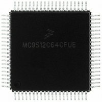
MC9S12C64CFUE Freescale Semiconductor, MC9S12C64CFUE Datasheet - Page 105

MC9S12C64CFUE
Manufacturer Part Number
MC9S12C64CFUE
Description
IC MCU 64K FLASH 4K RAM 80-QFP
Manufacturer
Freescale Semiconductor
Series
HCS12r
Specifications of MC9S12C64CFUE
Core Processor
HCS12
Core Size
16-Bit
Speed
25MHz
Connectivity
CAN, EBI/EMI, SCI, SPI
Peripherals
POR, PWM, WDT
Number Of I /o
60
Program Memory Size
64KB (64K x 8)
Program Memory Type
FLASH
Ram Size
4K x 8
Voltage - Supply (vcc/vdd)
2.35 V ~ 5.5 V
Data Converters
A/D 8x10b
Oscillator Type
Internal
Operating Temperature
-40°C ~ 85°C
Package / Case
80-QFP
Processor Series
S12C
Core
HCS12
Data Bus Width
16 bit
Data Ram Size
4 KB
Interface Type
CAN/SCI/SPI
Maximum Clock Frequency
25 MHz
Number Of Programmable I/os
60
Number Of Timers
8
Maximum Operating Temperature
+ 85 C
Mounting Style
SMD/SMT
3rd Party Development Tools
EWHCS12
Development Tools By Supplier
M68EVB912C32EE
Minimum Operating Temperature
- 40 C
On-chip Adc
8-ch x 10-bit
Package
80PQFP
Family Name
HCS12
Maximum Speed
25 MHz
Operating Supply Voltage
2.5|5 V
Height
2.4 mm
Length
14 mm
Supply Voltage (max)
2.75 V, 5.5 V
Supply Voltage (min)
2.35 V, 2.97 V
Width
14 mm
Lead Free Status / RoHS Status
Lead free / RoHS Compliant
Eeprom Size
-
Lead Free Status / Rohs Status
Lead free / RoHS Compliant
Available stocks
Company
Part Number
Manufacturer
Quantity
Price
Company:
Part Number:
MC9S12C64CFUE
Manufacturer:
Freescale Semiconductor
Quantity:
10 000
- Current page: 105 of 690
- Download datasheet (4Mb)
2.4.1.4
If the port is used as an output the register allows the configuration of the drive strength.
2.4.1.5
This register turns on a pull-up or pull-down device. It becomes only active if the pin is used as an input
or as a wired-or output.
2.4.1.6
This register selects either a pull-up or pull-down device if enabled. It becomes only active if the pin is
used as an input. A pull-up device can be activated if the pin is used as a wired-OR output.
2.4.2
2.4.2.1
This port is associated with the Standard Capture Timer. PWM output channels can be rerouted from port
P to port pins T. In all modes, port T pins can be used for either general-purpose I/O, Standard Capture
Timer I/O or as PWM channels module, if so configured by MODRR.
During reset, port T pins are configured as high-impedance inputs.
2.4.2.2
This port is associated with the serial SCI module. Port S pins PS[3:0] can be used either for general-
purpose I/O, or with the SCI subsystem.
During reset, port S pins are configured as inputs with pull-up.
2.4.2.3
This port is associated with the MSCAN and SPI module. Port M pins PM[5:0] can be used either for
general-purpose I/O, with the MSCAN or SPI subsystems.
During reset, port M pins are configured as inputs with pull-up.
2.4.2.4
This port is associated with the ATD module. Port AD pins can be used either for general-purpose I/O, or
for the ATD subsystem. There are 2 data port registers associated with the Port AD: PTAD[7:0], located
in the PIM and PORTAD[7:0] located in the ATD.
To use PTAD[n] as a standard input port, the corresponding DDRD[n] must be cleared. To use PTAD[n]
as a standard output port, the corresponding DDRD[n] must be set
NOTE: To use PORTAD[n], located in the ATD as an input port register, DDRD[n] must be cleared and
ATDDIEN[n] must be set. Please refer to ATD Block Guide for details.
Freescale Semiconductor
Port Descriptions
Reduced Drive Register
Pull Device Enable Register
Polarity Select Register
Port T
Port S
Port M
Port AD
MC9S12C-Family / MC9S12GC-Family
Rev 01.24
Chapter 2 Port Integration Module (PIM9C32) Block Description
105
Related parts for MC9S12C64CFUE
Image
Part Number
Description
Manufacturer
Datasheet
Request
R
Part Number:
Description:
Manufacturer:
Freescale Semiconductor, Inc
Datasheet:
Part Number:
Description:
Manufacturer:
Freescale Semiconductor, Inc
Datasheet:
Part Number:
Description:
Manufacturer:
Freescale Semiconductor, Inc
Datasheet:
Part Number:
Description:
Manufacturer:
Freescale Semiconductor, Inc
Datasheet:
Part Number:
Description:
Manufacturer:
Freescale Semiconductor, Inc
Datasheet:
Part Number:
Description:
Manufacturer:
Freescale Semiconductor, Inc
Datasheet:
Part Number:
Description:
Manufacturer:
Freescale Semiconductor, Inc
Datasheet:
Part Number:
Description:
Manufacturer:
Freescale Semiconductor, Inc
Datasheet:
Part Number:
Description:
Manufacturer:
Freescale Semiconductor, Inc
Datasheet:
Part Number:
Description:
Manufacturer:
Freescale Semiconductor, Inc
Datasheet:
Part Number:
Description:
Manufacturer:
Freescale Semiconductor, Inc
Datasheet:
Part Number:
Description:
Manufacturer:
Freescale Semiconductor, Inc
Datasheet:
Part Number:
Description:
Manufacturer:
Freescale Semiconductor, Inc
Datasheet:
Part Number:
Description:
Manufacturer:
Freescale Semiconductor, Inc
Datasheet:
Part Number:
Description:
Manufacturer:
Freescale Semiconductor, Inc
Datasheet:


