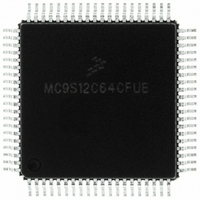
MC9S12C64CFUE Freescale Semiconductor, MC9S12C64CFUE Datasheet - Page 219

MC9S12C64CFUE
Manufacturer Part Number
MC9S12C64CFUE
Description
IC MCU 64K FLASH 4K RAM 80-QFP
Manufacturer
Freescale Semiconductor
Series
HCS12r
Specifications of MC9S12C64CFUE
Core Processor
HCS12
Core Size
16-Bit
Speed
25MHz
Connectivity
CAN, EBI/EMI, SCI, SPI
Peripherals
POR, PWM, WDT
Number Of I /o
60
Program Memory Size
64KB (64K x 8)
Program Memory Type
FLASH
Ram Size
4K x 8
Voltage - Supply (vcc/vdd)
2.35 V ~ 5.5 V
Data Converters
A/D 8x10b
Oscillator Type
Internal
Operating Temperature
-40°C ~ 85°C
Package / Case
80-QFP
Processor Series
S12C
Core
HCS12
Data Bus Width
16 bit
Data Ram Size
4 KB
Interface Type
CAN/SCI/SPI
Maximum Clock Frequency
25 MHz
Number Of Programmable I/os
60
Number Of Timers
8
Maximum Operating Temperature
+ 85 C
Mounting Style
SMD/SMT
3rd Party Development Tools
EWHCS12
Development Tools By Supplier
M68EVB912C32EE
Minimum Operating Temperature
- 40 C
On-chip Adc
8-ch x 10-bit
Package
80PQFP
Family Name
HCS12
Maximum Speed
25 MHz
Operating Supply Voltage
2.5|5 V
Height
2.4 mm
Length
14 mm
Supply Voltage (max)
2.75 V, 5.5 V
Supply Voltage (min)
2.35 V, 2.97 V
Width
14 mm
Lead Free Status / RoHS Status
Lead free / RoHS Compliant
Eeprom Size
-
Lead Free Status / Rohs Status
Lead free / RoHS Compliant
Available stocks
Company
Part Number
Manufacturer
Quantity
Price
Company:
Part Number:
MC9S12C64CFUE
Manufacturer:
Freescale Semiconductor
Quantity:
10 000
- Current page: 219 of 690
- Download datasheet (4Mb)
7.4.2.6
The DBG in DBG mode can operate in four capture modes. These modes are described in the following
subsections.
7.4.2.6.1
In normal mode, the DBG module uses comparator A and B as triggering devices. Change-of-flow
information or data will be stored depending on TRG in DBGSC.
7.4.2.6.2
The intent of loop1 mode is to prevent the trace buffer from being filled entirely with duplicate information
from a looping construct such as delays using the DBNE instruction or polling loops using
BRSET/BRCLR instructions. Immediately after address information is placed in the trace buffer, the DBG
module writes this value into the C comparator and the C comparator is placed in ignore address mode.
This will prevent duplicate address entries in the trace buffer resulting from repeated bit-conditional
branches. Comparator C will be cleared when the ARM bit is set in loop1 mode to prevent the previous
contents of the register from interfering with loop1 mode operation. Breakpoints based on comparator C
are disabled.
Loop1 mode only inhibits duplicate source address entries that would typically be stored in most tight
looping constructs. It will not inhibit repeated entries of destination addresses or vector addresses, because
repeated entries of these would most likely indicate a bug in the user’s code that the DBG module is
designed to help find.
LOOP
LOOP2 BRN
Freescale Semiconductor
INCX
BRCLR CMPTMP,#$0c,LOOP ; the BRCLR instruction also will be fetched by 1st P-cycle of BRCLR
NOP
DBNE
Capture Modes
*
A,LOOP2
Normal Mode
Loop1 Mode
In certain very tight loops, the source address will have already been fetched
again before the C comparator is updated. This results in the source address
being stored twice before further duplicate entries are suppressed. This
condition occurs with branch-on-bit instructions when the branch is fetched
by the first P-cycle of the branch or with loop-construct instructions in
which the branch is fetched with the first or second P cycle. See examples
below:
Loop1 mode does not support paged memory, and inhibits duplicate entries
in the trace buffer based solely on the CPU address. There is a remote
possibility of an erroneous address match if program flow alternates
between paged and unpaged memory space.
; 1-byte instruction fetched by 1st P-cycle of BRCLR
; 2-byte instruction fetched by 1st P-cycle of DBNE
; 1-byte instruction fetched by 2nd P-cycle of DBNE
; this instruction also fetched by 2nd P-cycle of DBNE
MC9S12C-Family / MC9S12GC-Family
Rev 01.24
NOTE
NOTE
Chapter 7 Debug Module (DBGV1) Block Description
219
Related parts for MC9S12C64CFUE
Image
Part Number
Description
Manufacturer
Datasheet
Request
R
Part Number:
Description:
Manufacturer:
Freescale Semiconductor, Inc
Datasheet:
Part Number:
Description:
Manufacturer:
Freescale Semiconductor, Inc
Datasheet:
Part Number:
Description:
Manufacturer:
Freescale Semiconductor, Inc
Datasheet:
Part Number:
Description:
Manufacturer:
Freescale Semiconductor, Inc
Datasheet:
Part Number:
Description:
Manufacturer:
Freescale Semiconductor, Inc
Datasheet:
Part Number:
Description:
Manufacturer:
Freescale Semiconductor, Inc
Datasheet:
Part Number:
Description:
Manufacturer:
Freescale Semiconductor, Inc
Datasheet:
Part Number:
Description:
Manufacturer:
Freescale Semiconductor, Inc
Datasheet:
Part Number:
Description:
Manufacturer:
Freescale Semiconductor, Inc
Datasheet:
Part Number:
Description:
Manufacturer:
Freescale Semiconductor, Inc
Datasheet:
Part Number:
Description:
Manufacturer:
Freescale Semiconductor, Inc
Datasheet:
Part Number:
Description:
Manufacturer:
Freescale Semiconductor, Inc
Datasheet:
Part Number:
Description:
Manufacturer:
Freescale Semiconductor, Inc
Datasheet:
Part Number:
Description:
Manufacturer:
Freescale Semiconductor, Inc
Datasheet:
Part Number:
Description:
Manufacturer:
Freescale Semiconductor, Inc
Datasheet:


