M30281F6HP#U3B Renesas Electronics America, M30281F6HP#U3B Datasheet - Page 300
M30281F6HP#U3B
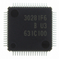
Manufacturer Part Number
M30281F6HP#U3B
Description
IC M16C/28 MCU FLASH 48K 64LQFP
Manufacturer
Renesas Electronics America
Series
M16C™ M16C/Tiny/28r
Datasheet
1.M30280F6HPU9.pdf
(425 pages)
Specifications of M30281F6HP#U3B
Core Processor
M16C/60
Core Size
16-Bit
Speed
20MHz
Connectivity
I²C, IEBus, SIO, UART/USART
Peripherals
DMA, POR, PWM, Voltage Detect, WDT
Number Of I /o
55
Program Memory Size
48KB (48K x 8)
Program Memory Type
FLASH
Ram Size
4K x 8
Voltage - Supply (vcc/vdd)
2.7 V ~ 5.5 V
Data Converters
A/D 13x10b
Oscillator Type
Internal
Operating Temperature
-40°C ~ 85°C
Package / Case
64-LQFP
For Use With
R0K330290S000BE - KIT EVAL STARTER FOR M16C/29M30290T2-CPE - EMULATOR COMPACT M16C/26A/28/29M30290T2-CPE-HP - EMULATOR COMPACT FOR M16C/TINY
Lead Free Status / RoHS Status
Lead free / RoHS Compliant
Eeprom Size
-
Available stocks
Company
Part Number
Manufacturer
Quantity
Price

Part Number:
M30281F6HP#U3BM30281F6HP#D5
Manufacturer:
Renesas Electronics America
Quantity:
10 000
Part Number:
M30281F6HP#U3BM30281F6HP#U3
Manufacturer:
Renesas Electronics America
Quantity:
10 000


R
R
M
e
E
1
. v
J
6
0
16.13.2 Example of Slave Receive
C
2
9
For example, a slave receives data as shown below when following conditions are met: high-speed clock
mode, SCL frequency of 400 kHz, ACK clock added and addressing format.
0 .
B
2 /
0
0
8
0
1) Set a slave address in the 7 high-order bits in the S0D0 register
2) Set "A5
3) Set “00
4) Set “08
5) When a START condition is received, addresses are compared
6) •When the transmitted addresses are all "0" (general call), the ADR0 bit in the S10 register is set to "1"
7) Write dummy data to the S00 register.
8) After receiving 1-byte data, an ACK-CLK bit is automatically returned and an I
9) To determine whether the ACK should be returned depending on contents in the received data, set
10) When receiving more than 1-byte control data, repeat steps 7) and 8) or 7) and 9).
11) When a STOP condition is detected, the communication is ended.
4
J
G
7
a
o r
0 -
•When the transmitted addresses match with the address set in 1), the ASS bit in the S10 register
•In other cases, the ADR0 and AAS bits are set to “0” and I
. n
S3D0 register to generate an ACK clock and set SCL clock frequency at 400kHz (f
interrupt request signal is generated.
dummy data to the S00 register to receive data after setting the WIT bit in te S3D0 register to "1"
(enable the I
interrupt is generated when the 1-byte data is received, set the ACKBIT bit to "1" or "0" to output a
signal from the ACKBIT bit.
and an I
is set to “1” and an I
is not generated.
u
2
3
0
p
, 1
0
(
M
2
0
16
16
16
1
0
2
6
7
" to the S20 register, “000
” to the S10 register to reset transmit/receive mode
” to the S1D0 register to enable data communication
C bus interface interrupt request signal is generated.
C
2 /
page 278
2
, 8
C bus interface interrupt of data receive completion). Because the I
M
1
6
C
2
f o
2 /
C bus interface interrupt request signal is generated.
8
3
) B
8
5
2
” to the ICK4 to ICK2 bits in the S4D0 register, and “00
2
16. MULTI-MASTER I
C bus interface interrupt request signal
2
2
2
C bus INTERFACE
C bus interface
C bus interface
1
=8MHz)
16
” to the
Related parts for M30281F6HP#U3B
Image
Part Number
Description
Manufacturer
Datasheet
Request
R

Part Number:
Description:
KIT STARTER FOR M16C/29
Manufacturer:
Renesas Electronics America
Datasheet:

Part Number:
Description:
KIT STARTER FOR R8C/2D
Manufacturer:
Renesas Electronics America
Datasheet:

Part Number:
Description:
R0K33062P STARTER KIT
Manufacturer:
Renesas Electronics America
Datasheet:

Part Number:
Description:
KIT STARTER FOR R8C/23 E8A
Manufacturer:
Renesas Electronics America
Datasheet:

Part Number:
Description:
KIT STARTER FOR R8C/25
Manufacturer:
Renesas Electronics America
Datasheet:

Part Number:
Description:
KIT STARTER H8S2456 SHARPE DSPLY
Manufacturer:
Renesas Electronics America
Datasheet:

Part Number:
Description:
KIT STARTER FOR R8C38C
Manufacturer:
Renesas Electronics America
Datasheet:

Part Number:
Description:
KIT STARTER FOR R8C35C
Manufacturer:
Renesas Electronics America
Datasheet:

Part Number:
Description:
KIT STARTER FOR R8CL3AC+LCD APPS
Manufacturer:
Renesas Electronics America
Datasheet:
Part Number:
Description:
KIT STARTER FOR RX610
Manufacturer:
Renesas Electronics America
Datasheet:

Part Number:
Description:
KIT STARTER FOR R32C/118
Manufacturer:
Renesas Electronics America
Datasheet:

Part Number:
Description:
KIT DEV RSK-R8C/26-29
Manufacturer:
Renesas Electronics America
Datasheet:

Part Number:
Description:
KIT STARTER FOR SH7124
Manufacturer:
Renesas Electronics America
Datasheet:

Part Number:
Description:
KIT STARTER FOR H8SX/1622
Manufacturer:
Renesas Electronics America
Datasheet:

Part Number:
Description:
KIT DEV FOR SH7203
Manufacturer:
Renesas Electronics America
Datasheet: