MC9S12D64CPVE Freescale Semiconductor, MC9S12D64CPVE Datasheet - Page 110
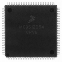
MC9S12D64CPVE
Manufacturer Part Number
MC9S12D64CPVE
Description
IC MCU 64K FLASH 25MHZ 112LQFP
Manufacturer
Freescale Semiconductor
Series
HCS12r
Specifications of MC9S12D64CPVE
Core Processor
HCS12
Core Size
16-Bit
Speed
25MHz
Connectivity
CAN, I²C, SCI, SPI
Peripherals
PWM, WDT
Number Of I /o
91
Program Memory Size
64KB (64K x 8)
Program Memory Type
FLASH
Eeprom Size
1K x 8
Ram Size
4K x 8
Voltage - Supply (vcc/vdd)
2.35 V ~ 5.25 V
Data Converters
A/D 16x10b
Oscillator Type
Internal
Operating Temperature
-40°C ~ 85°C
Package / Case
112-LQFP
Processor Series
S12D
Core
HCS12
Data Bus Width
16 bit
Data Ram Size
4 KB
Interface Type
CAN/I2C/SCI/SPI
Maximum Clock Frequency
25 MHz
Number Of Programmable I/os
49
Number Of Timers
8
Maximum Operating Temperature
+ 85 C
Mounting Style
SMD/SMT
3rd Party Development Tools
EWHCS12
Development Tools By Supplier
M68KIT912DP256
Minimum Operating Temperature
- 40 C
On-chip Adc
2 (8-ch x 10-bit)
Lead Free Status / RoHS Status
Lead free / RoHS Compliant
Available stocks
Company
Part Number
Manufacturer
Quantity
Price

Company:
Part Number:
MC9S12D64CPVE
Manufacturer:
Freescale Semiconductor
Quantity:
10 000
Part Number:
MC9S12D64CPVE
Manufacturer:
FREESCALE
Quantity:
20 000


MC9S12DJ64 Device User Guide — V01.20
The phase detector relationship is given by:
i
The loop bandwidth f
typical values are 50. = 0.9 ensures a good transient response.
And finally the frequency relationship is defined as
With the above values the resistance can be calculated. The example is shown for a loop bandwidth
f
The capacitance C
The capacitance C
A.5.3.2 Jitter Information
The basic functionality of the PLL is shown in Figure A-2. With each transition of the clock f
deviation from the reference clock f
accordingly.The adjustment is done continuously with no abrupt changes in the clock output frequency.
Noise, voltage, temperature and other factors cause slight variations in the control loop resulting in a clock
jitter. This jitter affects the real minimum and maximum clock periods as illustrated in Figure A-3.
ch
C
110
=10kHz:
is the current in tracking mode.
R
=
C
2
---------------------------- -
s
p
s
can now be calculated as:
should be chosen in the range of:
C
f
=
C
should be chosen to fulfill the Gardner’s stability criteria by at least a factor of 10,
K
n
<
--------------------- -
K
n f
2
------------------------------------------
C
=
f
C
s
C
=
f
------------ -
VCO
2
f
2
20 C
ref
–
R
= 2* *50*10kHz/(316.7Hz/ )=9.9k =~10k
+
ref
i
ch
is measured and input voltage to the VCO is adjusted
=
1
0.516
-------------- -
f
f
C
ref
p
+
2
K
R
V
2
C
;
synr
s
----- -
10
1
=
10
0.9
+
= 316.7Hz/
1
f
C
f
C
C
p
<
= 5.19nF =~ 4.7nF
< 25kHz
= 470pF
= 50
------------- -
4 10
f
ref
;
=
0.9
cmp
, the
Related parts for MC9S12D64CPVE
Image
Part Number
Description
Manufacturer
Datasheet
Request
R

Part Number:
Description:
Manufacturer:
Freescale Semiconductor, Inc
Datasheet:
Part Number:
Description:
Manufacturer:
Freescale Semiconductor, Inc
Datasheet:
Part Number:
Description:
Manufacturer:
Freescale Semiconductor, Inc
Datasheet:
Part Number:
Description:
Manufacturer:
Freescale Semiconductor, Inc
Datasheet:
Part Number:
Description:
Manufacturer:
Freescale Semiconductor, Inc
Datasheet:
Part Number:
Description:
Manufacturer:
Freescale Semiconductor, Inc
Datasheet:
Part Number:
Description:
Manufacturer:
Freescale Semiconductor, Inc
Datasheet:
Part Number:
Description:
Manufacturer:
Freescale Semiconductor, Inc
Datasheet:
Part Number:
Description:
Manufacturer:
Freescale Semiconductor, Inc
Datasheet:
Part Number:
Description:
Manufacturer:
Freescale Semiconductor, Inc
Datasheet:
Part Number:
Description:
Manufacturer:
Freescale Semiconductor, Inc
Datasheet:
Part Number:
Description:
Manufacturer:
Freescale Semiconductor, Inc
Datasheet:
Part Number:
Description:
Manufacturer:
Freescale Semiconductor, Inc
Datasheet:
Part Number:
Description:
Manufacturer:
Freescale Semiconductor, Inc
Datasheet:
Part Number:
Description:
Manufacturer:
Freescale Semiconductor, Inc
Datasheet: