MC9S12D64CPVE Freescale Semiconductor, MC9S12D64CPVE Datasheet - Page 13
MC9S12D64CPVE
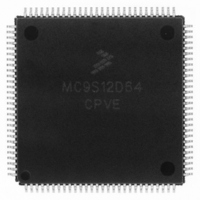
Manufacturer Part Number
MC9S12D64CPVE
Description
IC MCU 64K FLASH 25MHZ 112LQFP
Manufacturer
Freescale Semiconductor
Series
HCS12r
Specifications of MC9S12D64CPVE
Core Processor
HCS12
Core Size
16-Bit
Speed
25MHz
Connectivity
CAN, I²C, SCI, SPI
Peripherals
PWM, WDT
Number Of I /o
91
Program Memory Size
64KB (64K x 8)
Program Memory Type
FLASH
Eeprom Size
1K x 8
Ram Size
4K x 8
Voltage - Supply (vcc/vdd)
2.35 V ~ 5.25 V
Data Converters
A/D 16x10b
Oscillator Type
Internal
Operating Temperature
-40°C ~ 85°C
Package / Case
112-LQFP
Processor Series
S12D
Core
HCS12
Data Bus Width
16 bit
Data Ram Size
4 KB
Interface Type
CAN/I2C/SCI/SPI
Maximum Clock Frequency
25 MHz
Number Of Programmable I/os
49
Number Of Timers
8
Maximum Operating Temperature
+ 85 C
Mounting Style
SMD/SMT
3rd Party Development Tools
EWHCS12
Development Tools By Supplier
M68KIT912DP256
Minimum Operating Temperature
- 40 C
On-chip Adc
2 (8-ch x 10-bit)
Lead Free Status / RoHS Status
Lead free / RoHS Compliant
Available stocks
Company
Part Number
Manufacturer
Quantity
Price

Company:
Part Number:
MC9S12D64CPVE
Manufacturer:
Freescale Semiconductor
Quantity:
10 000
Part Number:
MC9S12D64CPVE
Manufacturer:
FREESCALE
Quantity:
20 000


List of Tables
Table 0-1
Table 0-2
Table 1-1
Table 1-2
Table 1-3
$0000 - $000F MEBI map 1 of 3 (HCS12 Multiplexed External Bus Interface) ................30
$0010 - $0014
$0015 - $0016
$0017 - $0019
$001A - $001B Device ID Register (Table 1-4) ................................................................31
$001C - $001D MMC map 3 of 4 (HCS12 Module Mapping Control, Table 1-5) ..............31
$001E - $001E MEBI map 2 of 3 (HCS12 Multiplexed External Bus Interface) ................31
$001F - $001F INT map 2 of 2 (HCS12 Interrupt) ............................................................32
$0020 - $0027
$0028 - $002F BKP (HCS12 Breakpoint) .........................................................................32
$0030 - $0031
$0032 - $0033
$0034 - $003F CRG (Clock and Reset Generator) ..........................................................33
$0040 - $007F ECT (Enhanced Capture Timer 16 Bit 8 Channels) .................................33
$0080 - $009F ATD0 (Analog to Digital Converter 10 Bit 8 Channel) ..............................36
$00A0 - $00C7 PWM (Pulse Width Modulator 8 Bit 8 Channel) .......................................37
$00C8 - $00CF SCI0 (Asynchronous Serial Interface) ......................................................39
$00D0 - $00D7 SCI1 (Asynchronous Serial Interface) ......................................................39
$00D8 - $00DF SPI0 (Serial Peripheral Interface) ............................................................40
$00E0 - $00E7 IIC (Inter IC Bus) ......................................................................................40
$00E8 - $00EF BDLC (Bytelevel Data Link Controller J1850) ..........................................41
$00F0 - $00FF Reserved ..................................................................................................41
$0100 - $010F Flash Control Register (fts64k) ................................................................41
$0110 - $011B EEPROM Control Register (eets1k) ........................................................42
$011C - $011F Reserved for RAM Control Register ........................................................42
$0120 - $013F ATD1 (Analog to Digital Converter 10 Bit 8 Channel) ..............................43
$0140 - $017F CAN0 (Freescale Scalable CAN - FSCAN) ..............................................44
$0180 - $023F Reserved ..................................................................................................46
Derivative Differences . . . . . . . . . . . . . . . . . . . . . . . . . . . . . . . . . . . . . . . . . . . . . .15
Document References . . . . . . . . . . . . . . . . . . . . . . . . . . . . . . . . . . . . . . . . . . . . . .17
Device Memory Map for MC9S12DJ64 . . . . . . . . . . . . . . . . . . . . . . . . . . . . . . . . .25
Device Memory Map for MC9S12D32 . . . . . . . . . . . . . . . . . . . . . . . . . . . . . . . . . .28
Detailed FSCAN Foreground Receive and Transmit Buffer Layout . . . . . . . . . . .45
MMC map 1 of 4 (HCS12 Module Mapping Control) ...............................30
INT map 1 of 2 (HCS12 Interrupt) ............................................................31
Reserved ..................................................................................................31
Reserved ..................................................................................................32
MMC map 4 of 4 (HCS12 Module Mapping Control) ...............................32
MEBI map 3 of 3 (HCS12 Multiplexed External Bus Interface) ................32
MC9S12DJ64 Device User Guide — V01.20
13
Related parts for MC9S12D64CPVE
Image
Part Number
Description
Manufacturer
Datasheet
Request
R

Part Number:
Description:
Manufacturer:
Freescale Semiconductor, Inc
Datasheet:
Part Number:
Description:
Manufacturer:
Freescale Semiconductor, Inc
Datasheet:
Part Number:
Description:
Manufacturer:
Freescale Semiconductor, Inc
Datasheet:
Part Number:
Description:
Manufacturer:
Freescale Semiconductor, Inc
Datasheet:
Part Number:
Description:
Manufacturer:
Freescale Semiconductor, Inc
Datasheet:
Part Number:
Description:
Manufacturer:
Freescale Semiconductor, Inc
Datasheet:
Part Number:
Description:
Manufacturer:
Freescale Semiconductor, Inc
Datasheet:
Part Number:
Description:
Manufacturer:
Freescale Semiconductor, Inc
Datasheet:
Part Number:
Description:
Manufacturer:
Freescale Semiconductor, Inc
Datasheet:
Part Number:
Description:
Manufacturer:
Freescale Semiconductor, Inc
Datasheet:
Part Number:
Description:
Manufacturer:
Freescale Semiconductor, Inc
Datasheet:
Part Number:
Description:
Manufacturer:
Freescale Semiconductor, Inc
Datasheet:
Part Number:
Description:
Manufacturer:
Freescale Semiconductor, Inc
Datasheet:
Part Number:
Description:
Manufacturer:
Freescale Semiconductor, Inc
Datasheet:
Part Number:
Description:
Manufacturer:
Freescale Semiconductor, Inc
Datasheet: