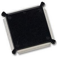
MC68331CEH25 Freescale Semiconductor, MC68331CEH25 Datasheet - Page 33

MC68331CEH25
Manufacturer Part Number
MC68331CEH25
Description
IC MCU 32BIT 25MHZ 132-PQFP
Manufacturer
Freescale Semiconductor
Series
M683xxr
Specifications of MC68331CEH25
Core Processor
CPU32
Core Size
32-Bit
Speed
25MHz
Connectivity
EBI/EMI, SCI, SPI, UART/USART
Peripherals
POR, PWM, WDT
Number Of I /o
18
Program Memory Type
ROMless
Voltage - Supply (vcc/vdd)
4.5 V ~ 5.5 V
Oscillator Type
Internal
Operating Temperature
-40°C ~ 85°C
Package / Case
132-QFP
Controller Family/series
68K
No. Of I/o's
18
Cpu Speed
25MHz
No. Of Timers
1
Embedded Interface Type
QSPI, SCI, UART
No. Of Pwm Channels
2
Digital Ic Case Style
PQFP
Rohs Compliant
Yes
Processor Series
M683xx
Core
CPU32
Data Bus Width
32 bit
Data Ram Size
80 B
Interface Type
QSPI, SCI, UART
Maximum Clock Frequency
25 MHz
Number Of Programmable I/os
18
Number Of Timers
1
Maximum Operating Temperature
+ 85 C
Mounting Style
SMD/SMT
Minimum Operating Temperature
- 40 C
Eeprom Size
-
Ram Size
-
Program Memory Size
-
Data Converters
-
Lead Free Status / Rohs Status
Details
Available stocks
Company
Part Number
Manufacturer
Quantity
Price
Company:
Part Number:
MC68331CEH25
Manufacturer:
PANASONIC
Quantity:
2 000
Company:
Part Number:
MC68331CEH25
Manufacturer:
Freescale Semiconductor
Quantity:
135
Company:
Part Number:
MC68331CEH25
Manufacturer:
Freescale Semiconductor
Quantity:
10 000
R/W —Read/Write
STRB —Address Strobe/Data Strobe
DSACK —Data and Size Acknowledge
MC68331TS/D
This field causes a chip select to be asserted only for a read, only for a write, or for both read and write.
Refer to the following table for options available.
This bit controls the timing for assertion of a chip select in asynchronous mode. Selecting address
strobe causes chip select to be asserted synchronized with address strobe. Selecting data strobe caus-
es chip select to be asserted synchronized with data strobe.
This field specifies the source of DSACK in asynchronous mode. It also allows the user to adjust bus
timing with internal DSACK generation by controlling the number of wait states that are inserted to op-
timize bus speed in a particular application. The following table shows the DSACK field encoding. The
fast termination encoding (1110) is used for two-cycle access to external memory.
0 = Address strobe
1 = Data strobe
Freescale Semiconductor, Inc.
For More Information On This Product,
Go to: www.freescale.com
DSACK
0000
0001
0010
0011
0100
0101
0110
0111
1000
1001
1010
1011
1100
1101
1110
1111
Byte
R/W
00
01
10
11
00
01
10
11
Fast Termination
External DSACK
No Wait States
10 Wait States
11 Wait States
12 Wait States
13 Wait States
2 Wait States
3 Wait States
4 Wait States
5 Wait States
6 Wait States
7 Wait States
8 Wait States
9 Wait States
Description
Description
Description
1 Wait State
Lower Byte
Upper Byte
Read/Write
Both Bytes
Read Only
Write Only
Reserved
Disable
33


