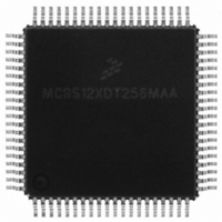
MC9S12XDT256MAA Freescale Semiconductor, MC9S12XDT256MAA Datasheet - Page 974

MC9S12XDT256MAA
Manufacturer Part Number
MC9S12XDT256MAA
Description
IC MCU 256K FLASH 80-QFP
Manufacturer
Freescale Semiconductor
Series
HCS12r
Datasheet
1.MC9S12XD64CAA.pdf
(1348 pages)
Specifications of MC9S12XDT256MAA
Core Processor
HCS12X
Core Size
16-Bit
Speed
80MHz
Connectivity
CAN, EBI/EMI, I²C, IrDA, LIN, SCI, SPI
Peripherals
LVD, POR, PWM, WDT
Number Of I /o
59
Program Memory Size
256KB (256K x 8)
Program Memory Type
FLASH
Eeprom Size
4K x 8
Ram Size
16K x 8
Voltage - Supply (vcc/vdd)
2.35 V ~ 5.5 V
Data Converters
A/D 8x10b
Oscillator Type
External
Operating Temperature
-40°C ~ 125°C
Package / Case
80-QFP
Cpu Family
HCS12
Device Core Size
16b
Frequency (max)
40MHz
Interface Type
CAN/I2C/SCI/SPI
Total Internal Ram Size
16KB
# I/os (max)
59
Number Of Timers - General Purpose
12
Operating Supply Voltage (typ)
2.5/5V
Operating Supply Voltage (max)
2.75/5.5V
Operating Supply Voltage (min)
2.35/3.15V
On-chip Adc
8-chx10-bit
Instruction Set Architecture
CISC
Operating Temp Range
-40C to 125C
Operating Temperature Classification
Automotive
Mounting
Surface Mount
Pin Count
80
Package Type
PQFP
Processor Series
S12XD
Core
HCS12
Data Bus Width
16 bit
Data Ram Size
16 KB
Maximum Clock Frequency
40 MHz
Number Of Programmable I/os
59
Number Of Timers
12
Operating Supply Voltage
0 V to 5.5 V
Maximum Operating Temperature
+ 125 C
Mounting Style
SMD/SMT
3rd Party Development Tools
EWHCS12
Development Tools By Supplier
EVB9S12XDP512E
Minimum Operating Temperature
- 40 C
Lead Free Status / RoHS Status
Lead free / RoHS Compliant
Available stocks
Company
Part Number
Manufacturer
Quantity
Price
Company:
Part Number:
MC9S12XDT256MAA
Manufacturer:
Freescale Semiconductor
Quantity:
10 000
- Current page: 974 of 1348
- Download datasheet (8Mb)
Chapter 24 DG128 Port Integration Module (S12XDG128PIMV2)
A standard port pin has the following minimum features:
Optional features:
24.0.2
Figure 24-1
976
•
•
•
•
•
•
•
•
•
•
•
•
•
•
•
•
•
•
•
•
Data and data direction registers for Ports A, B, E, K, T, S, M, P, H, J, and AD1 when used as
general-purpose I/O
Control registers to enable/disable pull-device and select pull-ups/pull-downs on Ports T, S, M, P,
H, and J on per-pin basis
Control registers to enable/disable pull-up devices on Port AD1 on per-pin basis
Single control register to enable/disable pull-ups on Ports A, B, E, and K on per-port basis and on
BKGD pin
Control registers to enable/disable reduced output drive on Ports T, S, M, P, H, J, and AD1 on per-
pin basis
Single control register to enable/disable reduced output drive on Ports A, B, E, and K on per-port
basis
Control registers to enable/disable open-drain (wired-OR) mode on Ports S and M
Control registers to enable/disable pin interrupts on Ports P, H, and J
Interrupt flag register for pin interrupts on Ports P, H, and J
Control register to configure IRQ pin operation
Free-running clock outputs
Input/output selection
5V output drive with two selectable drive strengths
5V digital and analog input
Input with selectable pull-up or pull-down device
Open drain for wired-OR connections
Interrupt inputs with glitch filtering
Reduced input threshold to support low voltage applications
Signals shown in Bold are not available in 80-pin packages.
Shaded labels denote alternative module routing ports.
Block Diagram
is a block diagram of the PIM.
MC9S12XDP512 Data Sheet, Rev. 2.21
Freescale Semiconductor
Related parts for MC9S12XDT256MAA
Image
Part Number
Description
Manufacturer
Datasheet
Request
R

Part Number:
Description:
16-BIT MICROPROCESSOR FAMILY
Manufacturer:
FREESCALE [Freescale Semiconductor, Inc]
Datasheet:
Part Number:
Description:
Manufacturer:
Freescale Semiconductor, Inc
Datasheet:
Part Number:
Description:
Manufacturer:
Freescale Semiconductor, Inc
Datasheet:
Part Number:
Description:
Manufacturer:
Freescale Semiconductor, Inc
Datasheet:
Part Number:
Description:
Manufacturer:
Freescale Semiconductor, Inc
Datasheet:
Part Number:
Description:
Manufacturer:
Freescale Semiconductor, Inc
Datasheet:
Part Number:
Description:
Manufacturer:
Freescale Semiconductor, Inc
Datasheet:
Part Number:
Description:
Manufacturer:
Freescale Semiconductor, Inc
Datasheet:
Part Number:
Description:
Manufacturer:
Freescale Semiconductor, Inc
Datasheet:
Part Number:
Description:
Manufacturer:
Freescale Semiconductor, Inc
Datasheet:
Part Number:
Description:
Manufacturer:
Freescale Semiconductor, Inc
Datasheet:
Part Number:
Description:
Manufacturer:
Freescale Semiconductor, Inc
Datasheet:
Part Number:
Description:
Manufacturer:
Freescale Semiconductor, Inc
Datasheet:
Part Number:
Description:
Manufacturer:
Freescale Semiconductor, Inc
Datasheet:
Part Number:
Description:
Manufacturer:
Freescale Semiconductor, Inc
Datasheet:


