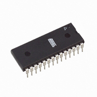
AT90LS4433-4PI Atmel, AT90LS4433-4PI Datasheet - Page 73

AT90LS4433-4PI
Manufacturer Part Number
AT90LS4433-4PI
Description
IC MCU 4K FLSH 4MHZ A/D LV 28DIP
Manufacturer
Atmel
Series
AVR® 90LSr
Datasheet
1.AT90S4433-8AC.pdf
(126 pages)
Specifications of AT90LS4433-4PI
Core Processor
AVR
Core Size
8-Bit
Speed
4MHz
Connectivity
SPI, UART/USART
Peripherals
Brown-out Detect/Reset, POR, PWM, WDT
Number Of I /o
20
Program Memory Size
4KB (2K x 16)
Program Memory Type
FLASH
Eeprom Size
256 x 8
Ram Size
128 x 8
Voltage - Supply (vcc/vdd)
2.7 V ~ 6 V
Data Converters
A/D 6x10b
Oscillator Type
External
Operating Temperature
-40°C ~ 85°C
Package / Case
28-DIP (0.300", 7.62mm)
Lead Free Status / RoHS Status
Contains lead / RoHS non-compliant
Port B as General Digital I/O
Alternate Functions of Port B
1042H–AVR–04/03
The Port B Input Pins address (PINB) is not a register; this address enables access to
the physical value on each Port B pin. When reading PORTB, the Port B Data Latch is
read, and when reading PINB, the logical values present on the pins are read.
All six pins in Port B have equal functionality when used as digital I/O pins.
PBn, general I/O pin: The DDBn bit in the DDRB Register selects the direction of this
pin. If DDBn is set (one), PBn is configured as an output pin. If DDBn is cleared (zero),
PBn is configured as an input pin. If PORTBn is set (one) when the pin is configured as
an input pin, the MOS pull-up resistor is activated. To switch the pull-up resistor off, the
PORTBn has to be cleared (zero) or the pin has to be configured as an output pin. The
port pins are tri-stated when a reset condition becomes active, even if the clock is not
running.
Table 24. DDBn Effects on Port B Pins
Note:
The alternate pin configuration is as follows:
• SCK – Port B, Bit 5
SCK: Master Clock output, Slave Clock input pin for SPI channel. When the SPI is
enabled as a Slave, this pin is configured as an input, regardless of the setting of DDB5.
When the SPI is enabled as a Master, the data direction of this pin is controlled by
DDB5. When the pin is forced to be an input, the pull-up can still be controlled by the
PORTB5 bit. See the description of the SPI port for further details.
• MISO – Port B, Bit 4
MISO: Master Data input, Slave Data output pin for SPI channel. When the SPI is
enabled as a Master, this pin is configured as an input, regardless of the setting of
DDB4. When the SPI is enabled as a Slave, the data direction of this pin is controlled by
DDB4. When the pin is forced to be an input, the pull-up can still be controlled by the
PORTB4 bit. See the description of the SPI port for further details.
• MOSI – Port B, Bit 3
MOSI: SPI Master Data output, Slave Data input for SPI channel. When the SPI is
enabled as a Slave, this pin is configured as an input, regardless of the setting of DDB3.
When the SPI is enabled as a Master, the data direction of this pin is controlled by
DDB3. When the pin is forced to be an input, the pull-up can still be controlled by the
PORTB3 bit. See the description of the SPI port for further details.
• SS – Port B, Bit 2
SS: Slave Port Select input. When the SPI is enabled as a Slave, this pin is configured
as an input, regardless of the setting of DDB2. As a Slave, the SPI is activated when this
pin is driven low. When the SPI is enabled as a Master, the data direction of this pin is
DDBn
0
0
1
1
1. n: 5..0, pin number.
PORTBn
0
1
0
1
Output
Output
Input
Input
I/O
Pull-up
Yes
No
No
No
(1)
Comment
Tri-state (high-Z)
PBn will source current if ext. pulled low.
Push-pull Zero Output
Push-pull One Output
AT90S/LS4433
73


