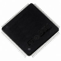
STR736FV2T7 STMicroelectronics, STR736FV2T7 Datasheet - Page 22

STR736FV2T7
Manufacturer Part Number
STR736FV2T7
Description
IC MCU ARM7 256K FLASH 100-TQFP
Manufacturer
STMicroelectronics
Series
STR7r
Datasheet
1.STR735FZ2T7.pdf
(52 pages)
Specifications of STR736FV2T7
Core Processor
ARM7
Core Size
32-Bit
Speed
36MHz
Connectivity
I²C, SPI, UART/USART
Peripherals
DMA, POR, PWM, WDT
Number Of I /o
72
Program Memory Size
256KB (256K x 8)
Program Memory Type
FLASH
Ram Size
16K x 8
Voltage - Supply (vcc/vdd)
4.5 V ~ 5.5 V
Data Converters
A/D 12x10b
Oscillator Type
Internal
Operating Temperature
-40°C ~ 105°C
Package / Case
100-TQFP, 100-VQFP
For Use With
497-5046 - KIT TOOL FOR ST7/UPSD/STR7 MCU
Lead Free Status / RoHS Status
Lead free / RoHS Compliant
Eeprom Size
-
Other names
497-5146-2
Available stocks
Company
Part Number
Manufacturer
Quantity
Price
Company:
Part Number:
STR736FV2T7
Manufacturer:
SONY
Quantity:
101
Company:
Part Number:
STR736FV2T7
Manufacturer:
STMicroelectronics
Quantity:
10 000
Electrical parameters
4.2
22/52
Absolute maximum ratings
Stresses above those listed as “absolute maximum ratings” may cause permanent damage
to the device. This is a stress rating only and functional operation of the device under these
conditions is not implied. Exposure to maximum rating conditions for extended periods may
affect device reliability.
Table 5.
Table 6.
1. All 5 V power (V
2. I
3. Negative injection disturbs the analog performance of the device. See note in
4. When several inputs are submitted to a current injection, the maximum
5.) In 144-pin devices, only +10 mA on P0.3, P1.13, P3.6 and P4.13 pins (negative injection not allowed).
I
INJ(PIN)
|V
V
ΣI
supply
cannot be respected, the injection current must be limited externally to the I
injection is induced by V
characteristics on page
positive and negative injected currents (instantaneous values). These results are based on
characterization with
V
V
INJ(PIN)
V
DDA
Symbol
Symbol
SSX
|ΔV
ESD(HBM)
INJ(PIN)
DD
ESD(MM)
V
I
I
VDD
VSS
V
I
SSA
IO
- V
DDx
- V
IN
- V
2) & 3)
must never be exceeded. This is implicitly insured if V
SSA
SS
SS
|
2)
Voltage characteristics
Current characteristics
|
DD
Total current into V
Total current out of V
Output current sunk by any I/O and control pin
Output current source by any I/O and control pin
Injected current on any other pin
Total injected current (sum of all I/O and control pins)
Input voltage on any pin
Variations between different 5 V
power pins
Variations between all the different
ground pins
Electrostatic discharge voltage
(Human Body Model)
Electrostatic discharge voltage
(Machine Model)
External 5 V Supply voltage
Reference ground for A/D converter
Reference voltage for A/D converter
, V
Σ
DDA
I
INJ(PIN)
43.
IN
) and ground (V
>V
DD
maximum current injection on four I/O port pins of the device.
while a negative injection is induced by V
Ratings
DD
SS
SS
power lines (source)
, V
ground lines (sink)
Ratings
SSA
) pins must always be connected to the external 5 V
4) &5)
(electrical sensitivity) on page 36
see
IN
maximum is respected. If V
1)
1)
: Absolute maximum ratings
Min
-0.3
-0.3
-0.3
V
-
-
SS
Σ
I
INJ(PIN)
IN
<V
INJ(PIN)
4)
Section 4.3.6: 10-bit ADC
SS
is the absolute sum of the
.
value. A positive
V
V
DD
DD
Max
V
6.0
0.3
0.3
SS
+0.3
+0.3
Max.
±10
±75
100
100
10
10
IN
maximum
STR73xFxx
Unit
Unit
mV
mA
V
V
V


