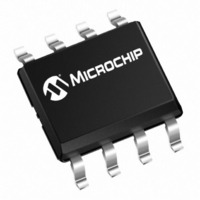
MCP6S92-E/MS Microchip Technology, MCP6S92-E/MS Datasheet - Page 19

MCP6S92-E/MS
Manufacturer Part Number
MCP6S92-E/MS
Description
IC PGA 2CH R-R I/O SPI 8MSOP
Manufacturer
Microchip Technology
Datasheet
1.MCP6S91-ESN.pdf
(40 pages)
Specifications of MCP6S92-E/MS
Amplifier Type
Programmable Gain
Number Of Circuits
2
Output Type
Rail-to-Rail
Slew Rate
22 V/µs
-3db Bandwidth
18MHz
Current - Input Bias
1pA
Voltage - Input Offset
400µV
Current - Supply
1mA
Current - Output / Channel
25mA
Voltage - Supply, Single/dual (±)
2.5 V ~ 5.5 V
Operating Temperature
-40°C ~ 125°C
Mounting Type
Surface Mount
Package / Case
8-MSOP, Micro8™, 8-uMAX, 8-uSOP,
For Use With
MCP6SX2DM-PCTLPD - BOARD DAUGHTER PICTAIL MCP6SX2
Lead Free Status / RoHS Status
Lead free / RoHS Compliant
Gain Bandwidth Product
-
Other names
MCP6S92-E/MSR
MCP6S92-E/MSR
MCP6S92-E/MSR
Available stocks
Company
Part Number
Manufacturer
Quantity
Price
Company:
Part Number:
MCP6S92-E/MS
Manufacturer:
Microchip
Quantity:
2 617
4.2.3
The maximum output voltage swing is the maximum
swing possible under a particular amplifier load current.
The amplifier load current is the sum of the external
load current (I
resistance (I
EQUATION 4-1:
FIGURE 4-2:
See Figure 2-21 for the typical output headroom
(V
load current.
The specification table states the output can reach
within 60 mV of either supply rail when R
V
4.2.4
The MCP6S91/2/3 amplifier family is designed with
CMOS input devices. It is designed to not exhibit phase
inversion when the input pins exceed the supply
voltages.
exceeding both supplies with no resulting phase
inversion.
The maximum voltage that can be applied to the input
pins (CHx) is V
the inputs that exceed this absolute maximum rating
can cause excessive current to flow into or out of the
input pins. Current beyond ±2 mA can cause possible
reliability problems. Applications that exceed this rating
must be externally limited with an input resistor, as
shown in Figure 4-3.
2004 Microchip Technology Inc.
REF
DD
= V
– V
Where:
DD
OH
Amplifier Load Current
Figure 2-29
RAIL-TO-RAIL OUTPUT
/2.
INPUT VOLTAGE AND PHASE
REVERSAL
LAD
or V
OUT
); see Figure 4-2.
SS
I
OL
LAD
) and the current through the ladder
– 0.3V to V
– V
=
Amplifier Load Current.
V
SS
-------------------------------------
REF
shows
V
) as a function of amplifier
OUT
I
R
OUT
I
LAD
LAD
R
DD
LAD
–
=
V
+ 0.3V. Voltages on
an
REF
I
OUT
V
OUT
input
+
L
I
= 10 k and
LAD
voltage
FIGURE 4-3:
into an input pin.
4.3
The
(R
switches in series with the inverting input reduces the
parasitic capacitance, distortion and gain mismatch.
R
causes additional current draw from the supplies. It is
also a load (Z
the V
In Shutdown mode, R
and V
fier’s inverting input are all connected through R
and the output is not High-Z (unlike the internal op
amp).
While R
small. Refer to Figure 2-12.
LAD
LAD
V
IN
REF
is an additional load on the output of the PGA and
REF
= R
R
R
resistor
LAD
IN
IN
Resistor Ladder
pin.
pins. Thus, these pins and the internal ampli-
F
+ R
contributes to the output noise, its effect is
(Maximum expected V
V
R
IN_REF
SS
G
IN
) sets the gain. Placing the gain
– (Maximum expected V
ladder
MCP6S91/2/3
) on the external circuitry driving
LAD
CHx
R
IN
MCP6S9X
is still attached to the V
2 mA
2 mA
limits the current flow
shown
IN
DS21908A-page 19
) – V
in
IN
DD
Figure 4-1
)
V
OUT
OUT
LAD


