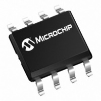
MCP6S92-E/MS Microchip Technology, MCP6S92-E/MS Datasheet - Page 20

MCP6S92-E/MS
Manufacturer Part Number
MCP6S92-E/MS
Description
IC PGA 2CH R-R I/O SPI 8MSOP
Manufacturer
Microchip Technology
Datasheet
1.MCP6S91-ESN.pdf
(40 pages)
Specifications of MCP6S92-E/MS
Amplifier Type
Programmable Gain
Number Of Circuits
2
Output Type
Rail-to-Rail
Slew Rate
22 V/µs
-3db Bandwidth
18MHz
Current - Input Bias
1pA
Voltage - Input Offset
400µV
Current - Supply
1mA
Current - Output / Channel
25mA
Voltage - Supply, Single/dual (±)
2.5 V ~ 5.5 V
Operating Temperature
-40°C ~ 125°C
Mounting Type
Surface Mount
Package / Case
8-MSOP, Micro8™, 8-uMAX, 8-uSOP,
For Use With
MCP6SX2DM-PCTLPD - BOARD DAUGHTER PICTAIL MCP6SX2
Lead Free Status / RoHS Status
Lead free / RoHS Compliant
Gain Bandwidth Product
-
Other names
MCP6S92-E/MSR
MCP6S92-E/MSR
MCP6S92-E/MSR
Available stocks
Company
Part Number
Manufacturer
Quantity
Price
Company:
Part Number:
MCP6S92-E/MS
Manufacturer:
Microchip
Quantity:
2 617
4.4
The V
impedance voltage source. The source driving the
V
0.1 to maintain reasonable gain accuracy. The supply
voltage V
R
circuit (Z
the gain. Any source driving the V
capable of driving a load as heavy as 0.16 k ||6 pF
(G = 32).
The absolute maximum voltages that can be applied to
the reference input pin (V
V
absolute maximum rating can cause excessive current
to flow into or out of this pin. Current beyond ±2 mA can
cause possible reliability problems. Because an
external series resistor cannot be used (for low gain
error), the external circuit must ensure that V
between V
The V
operation for the V
this region ensures proper operation of the PGA and its
surrounding circuitry.
4.5
These PGAs use a software shutdown command.
When the SPI interface sends a shutdown command,
the internal op amp is shut down and its output placed
in a High-Z state.
The resistive ladder is always connected between
V
output resistance will be on the order of 5 k , with a
path for output signals to appear at the input.
2004 Microchip Technology Inc.
REF
DD
REF
LAD
+ 0.3V. Voltages on the inputs that exceed this
and V
pin should have an output impedance less than
presents a load at the V
REF
IVR_REF
IN_REF
Rail-to-Rail V
Shutdown Mode
SS
SS
input is intended to be driven by a low-
OUT
and V
– 0.3V and V
; even in shutdown. This means that the
spec shows the region of normal
(5 k /G)||(6 pF)), which depends on
DD
REF
usually meet this requirement.
pin (V
REF
DD
REF
SS
+ 0.3V.
REF
Input
) are V
to V
pin to the external
DD
REF
). Staying within
SS
pin must be
– 0.3V and
REF
is
MCP6S91/2/3
DS21908A-page 20


