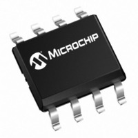
MCP6S92-E/MS Microchip Technology, MCP6S92-E/MS Datasheet - Page 8

MCP6S92-E/MS
Manufacturer Part Number
MCP6S92-E/MS
Description
IC PGA 2CH R-R I/O SPI 8MSOP
Manufacturer
Microchip Technology
Datasheet
1.MCP6S91-ESN.pdf
(40 pages)
Specifications of MCP6S92-E/MS
Amplifier Type
Programmable Gain
Number Of Circuits
2
Output Type
Rail-to-Rail
Slew Rate
22 V/µs
-3db Bandwidth
18MHz
Current - Input Bias
1pA
Voltage - Input Offset
400µV
Current - Supply
1mA
Current - Output / Channel
25mA
Voltage - Supply, Single/dual (±)
2.5 V ~ 5.5 V
Operating Temperature
-40°C ~ 125°C
Mounting Type
Surface Mount
Package / Case
8-MSOP, Micro8™, 8-uMAX, 8-uSOP,
For Use With
MCP6SX2DM-PCTLPD - BOARD DAUGHTER PICTAIL MCP6SX2
Lead Free Status / RoHS Status
Lead free / RoHS Compliant
Gain Bandwidth Product
-
Other names
MCP6S92-E/MSR
MCP6S92-E/MSR
MCP6S92-E/MSR
Available stocks
Company
Part Number
Manufacturer
Quantity
Price
Company:
Part Number:
MCP6S92-E/MS
Manufacturer:
Microchip
Quantity:
2 617
FIGURE 1-5:
1.1
1.1.1
The ideal PGA output voltage (V
EQUATION 1-1:
(see Figure 1-6). This equation holds when there are
no gain or offset errors and when the V
a low-impedance source (<< 0.1 ) at ground potential
(V
1.1.2
The PGA’s linear region of operation, including offset
and gain errors, is modeled by the line V
Figure 1-6.
EQUATION 1-2:
2004 Microchip Technology Inc.
Where:
SS
V
= 0V).
G is the nominal gain
O_LIN
V
SCK
REF
DC Output Voltage Specs / Model
V
SO
CS
SI
O_ID
IDEAL MODEL
LINEAR MODEL
=
=
G 1
V
=
SS
G
+
=
VIN
(first 16 bits out are always zeros)
g
0V
E
Detailed SPI™ Serial Interface Timing; SPI 1,1 Mode.
t
V
CSSC
IN
V
REF
–
t
0.3V
---------- -
SU
OUT
G
=
V
+
t
) is:
HD
SS
V
REF
OS
O_LIN
=
0V
pin is tied to
+
0.3V
shown in
t
HI
1/f
SCK
t
LO
The end points of this line are at V
V
the gain and offset specifications referred to in the
electrical specifications as follows:
EQUATION 1-3:
The DC Gain Drift ( G/ T
change in g
following equation:
EQUATION 1-4:
DD
– 0.3V. Figure 1-6 shows the relationship between
t
DO
V
OS
E
across temperature. This is shown in the
=
g
E
------------------------ -
G 1
=
t
MCP6S91/2/3
SCCS
G
V
100%
+
1
g
E
T
A
t
t
A
) can be calculated from the
CS1
SOZ
------------------------------------- -
G V
=
V
DD
--------- -
t
2
g
T
CSH
–
E
A
O_ID
–
V
G
0.6V
1
DS21908A-page 8
t
CS0
=
= 0.3V and
+1


