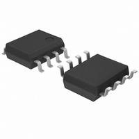
LM2904MX Rohm Semiconductor, LM2904MX Datasheet - Page 7

LM2904MX
Manufacturer Part Number
LM2904MX
Description
IC OPAMP DUAL 26V 8-SOIC
Manufacturer
Rohm Semiconductor
Series
Nowr
Specifications of LM2904MX
Amplifier Type
General Purpose
Number Of Circuits
2
Current - Input Bias
45nA
Voltage - Input Offset
2000µV
Current - Supply
1mA
Current - Output / Channel
40mA
Voltage - Supply, Single/dual (±)
3 V ~ 26 V, ±1.5 V ~ 13 V
Operating Temperature
-40°C ~ 85°C
Mounting Type
Surface Mount
Package / Case
8-SOIC (3.9mm Width)
Op Amp Type
General Purpose
No. Of Amplifiers
2
Supply Voltage Range
± 1.5V To ± 16V
Amplifier Case Style
SOIC
No. Of Pins
8
Operating Temperature Range
-40°C To +125°C
Svhc
No SVHC (18-Jun-2010)
Number Of Channels
2
Voltage Gain Db
100 dB
Common Mode Rejection Ratio (min)
50 dB
Input Offset Voltage
7 mV
Operating Supply Voltage
5 V, 9 V, 12 V, 15 V
Supply Current
1.2 mA
Maximum Power Dissipation
450 mW
Maximum Operating Temperature
+ 125 C
Mounting Style
SMD/SMT
Maximum Dual Supply Voltage
+/- 16 V
Minimum Operating Temperature
- 40 C
Lead Free Status / RoHS Status
Lead free / RoHS Compliant
Output Type
-
-3db Bandwidth
-
Slew Rate
-
Gain Bandwidth Product
-
Lead Free Status / Rohs Status
Details
Other names
LM2904MXTR
Available stocks
Company
Part Number
Manufacturer
Quantity
Price
Company:
Part Number:
LM2904MX
Manufacturer:
Fairchild Semiconductor
Quantity:
34 158
Part Number:
LM2904MX
Manufacturer:
NS/国半
Quantity:
20 000
Part Number:
LM2904MX/NOPB
Manufacturer:
TI/德州仪器
Quantity:
20 000
Derating curves
Precautions
1) Unused circuits
2) Input terminal voltage
3) Power supply (single / dual)
4) Power dissipation (Pd)
5) Short-circuit between pins and erroneous mounting
6) Operation in a strong electromagnetic field
7) Radiation
8) IC handing
9) IC operation
10) Board inspection
11) Output capacitor
When there are unused circuits, it is recommended that they be connected as
in Fig.7, setting the non-inverting input terminal to a potential within the
in-phase input voltage range (VICR).
Applying GND + 32V to the input terminal is possible without causing
deterioration of the electrical characteristics or destruction, irrespective of
the supply voltage. However, this does not ensure normal circuit operation.
Please note that the circuit operates normally only when the input voltage is
within the common mode input voltage range of the electric characteristics.
The op-amp operates when the voltage supplied is between V
Therefore, the single supply op-mp can be used as a dual supply op-amp as well.
Using the unit in excess of the rated power dissipation may cause deterioration in electrical characteristics due to the rise in chip temperature, including
reduced current capability. Therefore, please take into consideration the power dissipation (Pd) under actual operating conditions and apply a sufficient
margin in thermal design. Refer to the thermal derating curves for more information.
Incorrect mounting may damage the IC. In addition, the presence of foreign substances between the outputs, the output and the power supply, or the output
and GND may result in IC destruction.
Operation in a strong electromagnetic field may cause malfunctions.
This IC is not designed to withstand radiation.
Applying mechanical stress to the IC by deflecting or bending the board may cause fluctuation of the electrical characteristics due to piezoelectric (piezo)
effects.
The output stage of the IC is configured using Class C push-pull circuits. Therefore, when the load resistor is connected to the middle potential of V
GND, crossover distortion occurs at the changeover between discharging and charging of the output current. Connecting a resistor between the output
terminal and GND, and increasing the bias current for Class A operation will suppress crossover distortion.
Connecting a capacitor to a pin with low impedance may stress the IC. Therefore, discharging the capacitor after every process is recommended. In addition,
when attaching and detaching the jig during the inspection phase, ensure that the power is turned OFF before inspection and removal. Furthermore, please
take measures against ESD in the assembly process as well as during transportation and storage.
Discharge of the external output capacitor to V
due to thermal stress. Therefore, when using this IC in circuits where oscillation due to output capacitive load does not occur, such as in voltage comparators,
use an output capacitor with a capacitance less than 0.1 F.
1000
800
600
400
200
0
25
Ambient temperature : Ta [ ]
50
LM358MX
450[mV] S.O package8 (*5)
75
+
70[ ]
is possible via internal parasitic elements when V
Power Dissipation
100
S.O Package8 (*5)
ja = (Tj-Ta)/Pd[ /W]
125
Package
150
+
and GND
Fig.6 Derating Curves
7/8
Pd[W]
450
1000
800
600
400
200
0
ja [ /W]
3.6
+
is shorted to GND, causing damage to the internal circuitry
25
Ambient temperature : Ta [ ]
connect
to Vicm
50
LM2904MX
450[mV] S.O package8 (*5)
Fig.7 Disable circuit example
These Products are designed and produced by ROHM.
75
NOW SERIES LM2904/2902/358/324 family
85[ ]
100
125
V
GND
+
150
+
and


