AD603AQ Analog Devices Inc, AD603AQ Datasheet
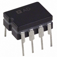
IC AMP VGA 90MHZ LN 50MA 8CDIP

AD603AQ

Manufacturer Part Number
AD603AQ
Description
IC AMP VGA 90MHZ LN 50MA 8CDIP
Manufacturer
Analog Devices Inc
Series
X-AMP®r
Datasheets

Specifications of AD603AQ

Rohs Status
RoHS non-compliant
Amplifier Type
Variable Gain
Number Of Circuits
1
Slew Rate
275 V/µs
-3db Bandwidth
90MHz
Current - Input Bias
200nA
Current - Supply
12.5mA
Current - Output / Channel
50mA
Voltage - Supply, Single/dual (±)
9.5 V ~ 12.6 V, ±4.75 V ~ 6.3 V
Operating Temperature
-40°C ~ 85°C
Mounting Type
Through Hole
Package / Case
8-CDIP (0.300", 7.62mm)
No. Of Amplifiers
1
Bandwidth
90MHz
Gain Accuracy
1.5dB
No. Of Channels
1
Supply Voltage Range
± 4.75V To ± 6.3V
Amplifier Case Style
DIP
No. Of Pins
8
Operating Temperature Range
-40°C To
Rohs Compliant
No
For Use With
AD603-EVALZ - BOARD EVALUATION FOR AD603
Output Type
-
Gain Bandwidth Product
-
Voltage - Input Offset
-
Lead Free Status / RoHS Status
Contains lead / RoHS non-compliant

Available stocks

Company
Part Number
Manufacturer
Quantity
Price
Part Number:
AD603AQ
Manufacturer:
AD
Quantity:
5 510
Part Number:
AD603AQ
Manufacturer:
XILINX
Quantity:
1 870
Part Number:
AD603AQ
Manufacturer:
ADI/亚德诺
Quantity:
20 000
a
PRODUCT DESCRIPTION
The AD603 is a low noise, voltage-controlled amplifier for use
in RF and IF AGC systems. It provides accurate, pin selectable
gains of –11 dB to +31 dB with a bandwidth of 90 MHz or 9 dB
to 51 dB with a bandwidth of 9 MHz. Any intermediate gain
range may be arranged using one external resistor. The input
referred noise spectral density is only 1.3 nV/÷Hz and power con-
sumption is 125 mW at the recommended ±5 V supplies.
The decibel gain is linear in dB, accurately calibrated, and stable
over temperature and supply. The gain is controlled at a high
impedance (50 MW), low bias (200 nA) differential input; the
*Patented.
REV. E
Information furnished by Analog Devices is believed to be accurate and
reliable. However, no responsibility is assumed by Analog Devices for its
use, nor for any infringements of patents or other rights of third parties that
may result from its use. No license is granted by implication or otherwise
under any patent or patent rights of Analog Devices. Trademarks and
registered trademarks are the property of their respective companies.
FEATURES
Linear in dB Gain Control
Pin Programmable Gain Ranges
Any Intermediate Range, e.g., –1 dB to +41 dB with
Bandwidth Independent of Variable Gain
1.3 nV/÷Hz Input Noise Spectral Density
MIL-STD-883 Compliant and DESC Versions Available
APPLICATIONS
RF/IF AGC Amplifier
Video Gain Control
A/D Range Extension
Signal Measurement
0.5 dB Typical Gain Accuracy
–11 dB to +31 dB with 90 MHz Bandwidth
9 dB to 51 dB with 9 MHz Bandwidth
30 MHz Bandwidth
COMM
GPOS
GNEG
VPOS
VNEG
VINP
0dB
V
R
G
REFERENCE
–6.02dB –12.04dB –18.06dB –24.08dB –30.1dB –36.12dB –42.14dB
SCALING
2R
INTERFACE
CONTROL
R
GAIN–
2R
R-2R LADDER NETWORK
R
FUNCTIONAL BLOCK DIAGRAM
2R
R
INPUT ATTENUATOR
2R
PRECISION PASSIVE
R
AD603
2R
scaling is 25 mV/dB, requiring a gain-control voltage of only 1 V to
span the central 40 dB of the gain range. An overrange and
underrange of 1 dB is provided whatever the selected range. The
gain-control response time is less than 1 ms for a 40 dB change.
The differential gain-control interface allows the use of either
differential or single-ended positive or negative control voltages.
Several of these amplifiers may be cascaded and their gain-
control gains offset to optimize the system S/N ratio.
The AD603 can drive a load impedance as low as 100 W with
low distortion. For a 500 W load in shunt with 5 pF, the total
harmonic distortion for a ± 1 V sinusoidal output at 10 MHz is
typically –60 dBc. The peak specified output is ± 2.5 V mini-
mum into a 500 W load, or ± 1 V into a 100 W load.
The AD603 uses a proprietary circuit topology—the X-AMP
The X-AMP comprises a variable attenuator of 0 dB to –42.14 dB
followed by a fixed-gain amplifier. Because of the attenuator,
the amplifier never has to cope with large inputs and can use
negative feedback to define its (fixed) gain and dynamic perfor-
mance. The attenuator has an input resistance of 100 W, laser
trimmed to ± 3%, and comprises a seven-stage R-2R ladder net-
work, resulting in an attenuation between tap points of 6.021 dB.
A proprietary interpolation technique provides a continuous
gain-control function which is linear in dB.
The AD603A is specified for operation from –40∞C to +85∞C and
is available in both 8-lead SOIC (R) and 8-lead ceramic CERDIP
(Q). The AD603S is specified for operation from –55∞C to
+125∞C and is available in an 8-lead ceramic CERDIP (Q).
The AD603 is also available under DESC SMD 5962-94572.
One Technology Way, P.O. Box 9106, Norwood, MA 02062-9106, U.S.A.
Tel: 781/329-4700
Fax: 781/326-8703
R
2R
R
R
Variable Gain Amplifier
*NORMAL VALUES
© 2003 Analog Devices, Inc. All rights reserved.
FIXED–GAIN
AMPLIFIER
Low Noise, 90 MHz
20 *
694 *
6.44k *
V
FDBK
OUT
AD603
www.analog.com
*
®
.

Related parts for AD603AQ

AD603AQ Summary of contents

Page 1

FEATURES Linear in dB Gain Control Pin Programmable Gain Ranges – +31 dB with 90 MHz Bandwidth with 9 MHz Bandwidth Any Intermediate Range, e.g., – +41 dB with 30 ...

Page 2

AD603–SPECIFICATIONS Model Parameter INPUT CHARACTERISTICS Input Resistance Input Capacitance 1 Input Noise Spectral Density Noise Figure 1 dB Compression Point Peak Input Voltage OUTPUT CHARACTERISTICS –3 dB Bandwidth Slew Rate 2 Peak Output Output Impedance Output Short-Circuit Current Group Delay ...

Page 3

... JA JC 8-Lead CERDIP Package 140∞C/ 15∞C Part Number AD603AR AD603AQ AD603SQ/883B* AD603-EB AD603ACHIPS AD603AR-REEL AD603AR-REEL7 *Refer to AD603 Military data sheet. Also available as 5962-9457203MPA. CAUTION ESD (electrostatic discharge) sensitive device. Electrostatic charges as high as 4000 V readily accumulate on the human body and test equipment and can discharge without detection. Although the AD603 features proprietary ESD protection circuitry, permanent damage may occur on devices subjected to high energy electrostatic discharges ...

Page 4

AD603 –Typical Performance Characteristics 2.50 45MHz 2.00 1.50 70MHz 1.00 10.7MHz 0.50 0.00 455kHz –0.50 70MHz –1.00 –1.50 –0.5 –0.4 –0.3 –0.2 –0.1 0.0 0.2 0.3 0.4 0.5 0.6 GAIN VOLTAGE (Volts) TPC 1. Gain Error vs. Gain Control Voltage ...

Page 5

FREQUENCY (Hz) TPC 10. Input Impedance vs. Frequency (Gain = –10 dB) 1V 100 200ns TPC 13. Gain-Control Channel Response Time 3.5V INPUT GND 500mV/DIV 500mV OUTPUT ...

Page 6

AD603 +5V 0.1 F HP3326A DUAL CHANNEL HP3585A 50 SYNTHESIZER AD603 SPECTRUM 100 ANALYZER 0.1 F –5V DATEL DVC 8500 TPC 19. Test Setup Used for: Noise Figure, Third Order Intercept and 1 dB Compression Point Measurements ...

Page 7

THEORY OF OPERATION The AD603 comprises a fixed-gain amplifier, preceded by a broadband passive attenuator 42.14 dB, having a gain-control scaling factor per volt. The fixed gain is laser-trimmed in two ranges, to ...

Page 8

AD603 The Gain-Control Interface The attenuation is controlled through a differential, high impedance (50 MW) input, with a scaling factor which is laser-trimmed per volt, that is, 25 mV/dB. An internal band gap reference ensures stability of ...

Page 9

Optionally, when a resistor is placed from FDBK to COMM, higher gains can be achieved. This fourth mode is of limited value because of the low bandwidth and the elevated output off- sets thus not included in Figure ...

Page 10

AD603 INPUT 0dB GPOS INPUT 0dB GPOS V = 1.0V C INPUT 0dB GPOS V = 2.0V C Figure 6. AD603 Gain Control Input Calculations for Sequential Control Operation +31.07dB +31.07dB A1 * +10dB * –11.07dB ...

Page 11

V C Figure 9. SNR for Cascaded Stages—Sequential Control 2.0 1.5 1.0 0.5 0.0 –0.5 –1.0 –1.5 –2.0 –0.2 0.0 0.2 0.4 0.6 0.8 1.0 1.2 1.4 ...

Page 12

AD603 3.0 2.5 2.0 1.5 1.0 0.5 0.0 –0.5 –1.0 –1.5 –2.0 –2.5 –3.0 –0.1 0.0 0.1 0.2 0.3 0.4 0.5 0 Figure 13. Gain Error for Cascaded Stages— Low Ripple Mode ...

Page 13

The automatic gain control voltage, V time integral of this error current. In order for V thus the gain) to remain insensitive to short-term amplitude fluctuations in the output signal, the rectified current in Q1 must, on average, ...

Page 14

AD603 OUTLINE DIMENSIONS 8-Lead Ceramic Dual In-Line Package [CERDIP] (Q-8) Dimensions shown in inches and (millimeters) 0.005 (0.13) 0.055 (1.40) MIN MAX 8 5 0.310 (7.87) 0.220 (5.59) PIN 0.100 (2.54) BSC 0.405 (10.29) MAX 0.060 (1.52) ...

Page 15

Revision History Location 8/03 Data Sheet changed from REV REV. E. Updated Format ............................................................................................................................................................... Changes to SPECIFICATIONS .......................................................................................................................................... 2 Changes to TPCs ..................................................................................................................................................... 4 Changes to Sequential Mode (Optimal S/N Ratio) section ................................................................................................... 9 Change ...

Page 16

–16– ...

Related keywords