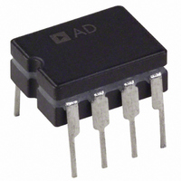
AD603AQ Analog Devices Inc, AD603AQ Datasheet - Page 8

AD603AQ
Manufacturer Part Number
AD603AQ
Description
IC AMP VGA 90MHZ LN 50MA 8CDIP
Manufacturer
Analog Devices Inc
Series
X-AMP®r
Specifications of AD603AQ
Rohs Status
RoHS non-compliant
Amplifier Type
Variable Gain
Number Of Circuits
1
Slew Rate
275 V/µs
-3db Bandwidth
90MHz
Current - Input Bias
200nA
Current - Supply
12.5mA
Current - Output / Channel
50mA
Voltage - Supply, Single/dual (±)
9.5 V ~ 12.6 V, ±4.75 V ~ 6.3 V
Operating Temperature
-40°C ~ 85°C
Mounting Type
Through Hole
Package / Case
8-CDIP (0.300", 7.62mm)
No. Of Amplifiers
1
Bandwidth
90MHz
Gain Accuracy
1.5dB
No. Of Channels
1
Supply Voltage Range
± 4.75V To ± 6.3V
Amplifier Case Style
DIP
No. Of Pins
8
Operating Temperature Range
-40°C To
Rohs Compliant
No
For Use With
AD603-EVALZ - BOARD EVALUATION FOR AD603
Output Type
-
Gain Bandwidth Product
-
Voltage - Input Offset
-
Lead Free Status / RoHS Status
Contains lead / RoHS non-compliant
Available stocks
Company
Part Number
Manufacturer
Quantity
Price
Part Number:
AD603AQ
Manufacturer:
ADI/亚德诺
Quantity:
20 000
AD603
The Gain-Control Interface
The attenuation is controlled through a differential, high
impedance (50 MW) input, with a scaling factor which is
laser-trimmed to 40 dB per volt, that is, 25 mV/dB. An internal
band gap reference ensures stability of the scaling with respect
to supply and temperature variations.
When the differential input voltage V
slider is centered, providing an attenuation of 21.07 dB. For the
maximum bandwidth range, this results in an overall gain of
10 dB (= –21.07 dB + 31.07 dB). When the control input is
–500 mV, the gain is lowered by 20 dB (= 0.500 V ¥ 40 dB/V),
to –10 dB; when set to +500 mV, the gain is increased by 20 dB, to
30 dB. When this interface is overdriven in either direction, the
gain approaches either –11.07 dB (= – 42.14 dB + 31.07 dB) or
31.07 dB (= 0 + 31.07 dB), respectively. The only constraint on
the gain-control voltage is that it be kept within the common-mode
range (–1.2 V to +2.0 V assuming +5 V supplies) of the gain
control interface.
The basic gain of the AD603 can thus be calculated using the
following simple expression:
where V
section), the gain becomes
and
The high impedance gain-control input ensures minimal loading
when driving many amplifiers in multiple channel or cascaded
applications. The differential capability provides flexibility in
choosing the appropriate signal levels and polarities for various
control schemes.
For example, if the gain is to be controlled by a DAC providing
a positive only ground-referenced output, the Gain Control
Low (GNEG) pin should be biased to a fixed offset of 500 mV, to
set the gain to –10 dB when Gain Control High (GPOS) is at
zero, and to 30 dB when at 1.00 V.
It is a simple matter to include a voltage divider to achieve other
scaling factors. When using an 8-bit DAC having an FS output
of 2.55 V (10 mV/bit), a divider ratio of 2 (generating 5 mV/bit)
would result in a gain-setting resolution of 0.2 dB/bit. The use
of such offsets is valuable when two AD603s are cascaded, when
various options exist for optimizing the S/N profile, as will be
shown later.
Programming the Fixed-Gain Amplifier Using Pin Strapping
Access to the feedback network is provided at Pin 5 (FDBK).
The user may program the gain of the AD603’s output amplifier
using this pin, as shown in Figure 2. There are three modes: in
the default mode, FDBK is unconnected, providing the range
+9 dB/+51 dB; when V
lowered to –11 dB/+31 dB; when an external resistor is placed
between V
for example, –1 dB/+41 dB. Figure 3 shows the nominal maxi-
mum gain versus external resistor for this mode.
Gain (dB) = 40 V
Gain (dB) = 40 V
Gain (dB) = 40 V
G
is in volts. When Pins 5 and 7 are strapped (see next
OUT
and FDBK any intermediate gain can be achieved,
G
G
G
OUT
+ 30 for +10 to +50 dB
+ 10
+ 20 for 0 to +40 dB
and FDBK are shorted, the gain is
G
= 0 V, the attenuator
(1)
(2)
–8–
Figure 3. Gain vs. R
Assuming Internal Resistors Have a Maximum Tolerance
of 20%
52
50
48
46
44
42
40
38
36
34
32
30
V
V
V
IN
IN
IN
10
a. –10 dB to +30 dB; 90 MHz Bandwidth
b. 0 dB to 40 dB; 30 MHz Bandwidth
c. 10 dB to 50 dB; 9 MHz Bandwidth
Figure 2. Pin Strapping to Set Gain
VC1
VC2
VC1
VC2
VC1
VC2
100
EXT
GPOS
GNEG
VINP
COMM
GPOS
GNEG
VINP
COMM
GPOS
GNEG
VINP
COMM
VdB (OUT)
–1:VdB (OUT)
AD603
AD603
AD603
, Showing Worst-Case Limits
1k
R
VPOS
VNEG
FDBK
VPOS
VNEG
FDBK
VPOS
VNEG
FDBK
V
V
V
EXT
OUT
OUT
OUT
( )
–2:VdB (OUT)
10k
VPOS
VNEG
VPOS
VNEG
VPOS
VNEG
18pF
100k
2.15k
5.6pF
V
V
V
OUT
OUT
OUT
1M
REV. E


