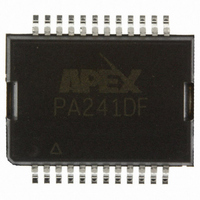
PA241DF Cirrus Logic Inc, PA241DF Datasheet - Page 3

PA241DF
Manufacturer Part Number
PA241DF
Description
OP AMP HV 350V .06A 24-PSOP DF
Manufacturer
Cirrus Logic Inc
Series
Apex Precision Power™r
Specifications of PA241DF
Amplifier Type
Power
Number Of Circuits
1
Slew Rate
30 V/µs
Gain Bandwidth Product
3MHz
Current - Input Bias
50pA
Voltage - Input Offset
25000µV
Current - Supply
2.2mA
Current - Output / Channel
120mA
Voltage - Supply, Single/dual (±)
100 V ~ 350 V, ±50 V ~ 175 V
Operating Temperature
-25°C ~ 85°C
Mounting Type
Surface Mount
Package / Case
24-PSOP
Number Of Channels
1
Voltage Gain Db
96 dB
Common Mode Rejection Ratio (min)
84 dB
Input Offset Voltage
40 mV
Maximum Operating Temperature
+ 85 C
Mounting Style
SMD/SMT
Maximum Dual Supply Voltage
+/- 175 V
Minimum Operating Temperature
- 25 C
For Use With
598-1459 - EVALUATION KIT FRO PA241DF
Lead Free Status / RoHS Status
Lead free / RoHS Compliant
Output Type
-
-3db Bandwidth
-
Lead Free Status / Rohs Status
Details
Other names
598-1357
Available stocks
Company
Part Number
Manufacturer
Quantity
Price
Part Number:
PA241DF
Manufacturer:
APEX
Quantity:
20 000
ABSOLUTE MAXIMUM RATINGS
PARAMETER
INPUT
OFFSET VOLTAGE, initial
OFFSET VOLTAGE, vs. temperature
OFFSET VOLTAGE, vs. temperature
OFFSET VOLTAGE, vs supply
OFFSET VOLTAGE, vs time
BIAS CURRENT, initial
BIAS CURRENT, vs supply
OFFSET CURRENT, initial
INPUT IMPEDANCE, DC
INPUT CAPACITANCE
COMMON MODE, voltage range
COMMON MODE, voltage range
COMMON MODE REJECTION, DC
NOISE, broad band
NOISE, low frequency
GAIN
OPEN LOOP at 15Hz
BANDWIDTH, gain bandwidth product
POWER BANDWIDTH
OUTPUT
VOLTAGE SWING
CURRENT, peak
CURRENT, continuous
SETTLING TIME to .1%
SLEW RATE
RESISTANCE
RESISTANCE
POWER SUPPLY
VOLTAGE
CURRENT, quiescent
THERMAL
PA241DW RESISTANCE, AC junction to case
PA241DW RESISTANCE, DC junction to case
PA241DW RESISTANCE, junction to air
TEMPERATURE RANGE, case
NOTES:
PA241U
SPECIFICATIONS
CAUTION
2.
3.
4.
5.
1.
*
5
5
, 1mA
, 40 mA
"A" specification is the same as the non "A" specification.
Unless otherwise noted T
rating.
Long term operation at the maximum junction temperature will result in reduced product life. Derate internal power dissipation
to achieve high MTTF. For guidance, refer to heatsink data sheet.
Sample tested by wafer to 95%.
Guaranteed but not tested.
The selected value of R
4
The PA241 is constructed from MOSFET transistors. ESD handling procedures must be observed.
P r o d u c t I n n o v a t i o n F r o m
3
3
CL
C
must be added to the values given for total output resistance.
= 25°C, C
25° to 85°C
-25° to 25°C
TEST CONDITIONS
V
10kHz BW, R
1-10 Hz
R
280V p-p
I
10V step, A
C
R
R
F > 60Hz
F < 60Hz
Full temperature range
Meets full range spec's
O
SUPPLY VOLTAGE, +V
OUTPUT CURRENT, continuous within SOA
OUTPUT CURRENT, peak
POWER DISSIPATION, continuous @ T
INPUT VOLTAGE, differential
INPUT VOLTAGE, common mode
TEMPERATURE, pin solder – 10 sec
TEMPERATURE, junction
TEMPERATURE, storage
TEMPERATURE RANGE, powered (case)
CM
L
C
CL
CL
= 40mA
= 5K
= 3.3pF
= ±90V DC
= 0
= 0
C
= 6.8pF. DC input specifications are ± value given. Power supply voltage is typical
V
S
= –10
= 1K
1
+V
±V
-V
S
MIN
120
±50
–25
to –V
84
90
60
S
S
S
+12
2
–14
–12
S
PA241DW
±V
±150
TYP
100
270
100
100
125
150
10
2.2
25
70
15
94
50
96
30
30
12
55
S
3
6
3
2
5
7
–10
11
C
= 25°C
MAX
2000
±175
250
500
400
+85
130
2.5
40
50
10
14
±V
MIN
PA241DW
PA241DWA
350V
60 mA
120 mA
9W
±16 V
±V
220°C
150°C
–65 to +150°C
–40 to +125°C
S
*
*
*
*
*
*
*
*
–10
S
PA241DWA
±V
TYP
15
S
*
*
*
*
*
*
*
*
*
*
*
*
*
*
*
*
*
*
*
*
*
*
*
*
–8.5
MAX
2.3
30
*
*
*
*
*
*
*
*
*
PA241
µV RMS
UNITS
µV p-p
µV/°C
µV/°C
µV/kh
°C/W
°C/W
°C/W
µV/V
pA/V
MHz
V/µs
kHz
mV
mA
mA
mA
pA
pA
dB
dB
pF
µs
°C
V
V
V
Ω
Ω
V
3


