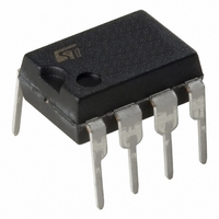
TL072IN STMicroelectronics, TL072IN Datasheet - Page 5

TL072IN
Manufacturer Part Number
TL072IN
Description
IC OP AMP JFET DUAL LNOISE 8-DIP
Manufacturer
STMicroelectronics
Specifications of TL072IN
Amplifier Type
J-FET
Number Of Circuits
2
Slew Rate
16 V/µs
Gain Bandwidth Product
4MHz
Current - Input Bias
20pA
Voltage - Input Offset
3000µV
Current - Supply
1.4mA
Current - Output / Channel
40mA
Voltage - Supply, Single/dual (±)
6 V ~ 36 V, ±3 V ~ 18 V
Operating Temperature
-40°C ~ 105°C
Mounting Type
Through Hole
Package / Case
8-DIP (0.300", 7.62mm)
Number Of Channels
2
Common Mode Rejection Ratio (min)
80 dB
Input Offset Voltage
10 mV
Input Bias Current (max)
200 pA
Supply Current
2.5 mA
Maximum Power Dissipation
680 mW
Maximum Operating Temperature
+ 105 C
Minimum Operating Temperature
- 40 C
Dual Supply Voltage
+/- 5 V, +/- 9 V, +/- 12 V, +/- 15 V
Maximum Dual Supply Voltage
+/- 18 V
Minimum Dual Supply Voltage
+/- 3 V
Mounting Style
Through Hole
Shutdown
No
Technology
BiFET
Voltage Gain Db
106.02 dB
Bandwidth
4 MHz
Channel Separation
120
Common Mode Rejection Ratio
86
Current, Input Bias
20 pA
Current, Input Offset
5 pA
Current, Output
20 mA
Current, Supply
1.4 mA
Harmonic Distortion
0.01 %
Number Of Amplifiers
Dual
Package Type
DIP-8
Resistance, Input
10^12 Ohms
Signal Gain
200 V/mV
Temperature, Operating, Range
-40 to +105 °C
Time, Rise
0.1 μs
Voltage, Input
±15 V
Voltage, Noise
15 nV/sqrt Hz
Voltage, Offset
3 mV
Voltage, Supply
6 to 36 V
Lead Free Status / RoHS Status
Lead free / RoHS Compliant
Output Type
-
-3db Bandwidth
-
Lead Free Status / Rohs Status
Lead free / RoHS Compliant
Other names
497-7659-5
TL072IN
TL072IN
00022-1,00053-1
Operating Temp range
Note5.
Note6.
Note7.
[2] Circuit Diagram
Storage Temp range
[3] Absolute Maximum Ratings
CN1-3,4,5
CN1-1
CN1-2
GND
TDK CORPORATION
Humidity range
Vin
N.C
Output Power
Input Voltage
If the start up voltage falls below Cold Cathode Tube strike voltage, the CCFL will not light up easily specially at
lower ambient temperature. Please review mounting instruction to avoid any abnor mal operation due to
coupling/leakage capacitance of inverter high voltage area to any surrounding conductor.
For operation in non-isolated configuration, please connect CN2-3 (V-Low) to input return (gro und) as the output of
DC/AC inverter is electrically isolated from input.
For proper operation of circuit protection (FUSE or IC PROTECTOR) of CXA-L0505- NJL, please use minimum of
2A capacity for input power supply and 1.0A for CXA-L0512-NJL and CXA-L0524-NJL.
Items
F1
Symbols
Pout
L1
Vin
RH
Ta
Ts
J1
R1
R2
R3
R4
L0505-NJL
-30~85
No.
0~60
0~6
3.5
95
PRODUCT DRAWING
NAME OF DRAWING
MATERIALS NAME
Specifications
L0512-NJL
-30~85
0~14.4
Q1
0~60
3.5
95
Q2
DC-AC INVERTER UNIT CXA-L05xx-NJL
J3
L0524-NJL
PRODUCT NAME or MODEL,TITLE
-30~85
0~28.8
0~60
3.5
95
J4
C2
C1
QU
%RH
Unit
Vdc
°C
W
C4
MATERIAL
A Maximum wet ball temperature is
J5
DRAWING No.
CTR-0732-E
T1
TSB-08-01-05(00) form-6(A4)
Notes
38°C.
C3
REMARK
CN2-1
CN2-3
Vin
Vin
PAGE
4


