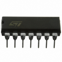
TS27M4IN STMicroelectronics, TS27M4IN Datasheet

TS27M4IN
Specifications of TS27M4IN
Related parts for TS27M4IN
TS27M4IN Summary of contents
Page 1
Precision low power CMOS quad operational amplifiers Features ■ Low power consumption: 150 µA/op ■ Output voltage can swing to ground ■ Excellent phase margin on capacitive loads ■ Unity gain stable ■ Two input offset voltage selections Description These ...
Page 2
Circuit schematics 1 Circuit schematics Figure 1. Block diagram Current source 2/ Input differential E E TS27M4C, TS27M4I, TS27M4M Output Second stage stage V CC Output V CC ...
Page 3
TS27M4C, TS27M4I, TS27M4M Figure 2. Schematic diagram (for 1/4 TS27M4) Circuit schematics 3/14 ...
Page 4
Absolute maximum ratings and operating conditions 2 Absolute maximum ratings and operating conditions Table 1. Absolute maximum ratings (AMR) Symbol Parameter ( Supply voltage CC V Differential input voltage id (3) V Input voltage in I Output current ...
Page 5
TS27M4C, TS27M4I, TS27M4M 3 Electrical characteristics + Table + Symbol Parameter Input offset voltage V = 1.4V TS27M4C/I/M V TS27M4AC/AI/AM io ≤ T ≤ min amb ...
Page 6
Electrical characteristics + Table + Symbol Parameter Phase margin at unity gain φ 40dB 100kΩ Overshoot factor OV Equivalent input noise voltage e n ...
Page 7
TS27M4C, TS27M4I, TS27M4M Figure 3. Supply current (each amplifier) versus supply voltage 200 ˚ AMB 150 O CC 100 SUPPLY VOLTAGE, V Figure ...
Page 8
Electrical characteristics Figure 9. Open loop frequency response and phase shift 50 40 GAIN 30 PHASE 25˚C amb + V = 10V 100k Ω 100pF Gain L 0 Bandwidth A ...
Page 9
... These packages have a lead-free second level interconnect. The category of second level interconnect is marked on the package and on the inner box label, in compliance with JEDEC Standard JESD97. The maximum ratings related to soldering conditions are also marked on the inner box label. ECOPACK is an STMicroelectronics trademark. ECOPACK specifications are available at: www.st.com. 4.1 DIP14 package information Figure 15 ...
Page 10
Package information 4.2 SO-14 package information Figure 16. SO-14 package mechanical drawing Table 5. SO-14 package mechanical data Ref 10/14 Dimensions Millimeters Min. Typ. ...
Page 11
TS27M4C, TS27M4I, TS27M4M 4.3 TSSOP14 package information Figure 17. TSSOP14 package mechanical drawing A PIN 1 IDENTIFICATION Figure 18. TSSOP14 package mechanical data Ref ...
Page 12
... Tube or Tape & reel 27M4AC TS27M4CN Tube TS27M4ACN 27M4C Tape & reel 27M4AC 27M4I Tube or Tape & reel 27M4AI TS27M4IN Tube TS27M4AIN 27M4I Tape & reel 27M4AI 27M4M Tube or Tape & reel 27M4AM TS27M4MN Tube TS27M4AMN 27M4M Tape & reel ...
Page 13
TS27M4C, TS27M4I, TS27M4M 6 Revision history Table 7. Document revision history Date 07-Jan-2001 08-Sep-2008 Revision 1 Initial release. Removed TS27M4B version of device. Added and ESD parameters in thja thjc maximum ratings (AMR). 2 Expanded Table ...
Page 14
... Information in this document is provided solely in connection with ST products. STMicroelectronics NV and its subsidiaries (“ST”) reserve the right to make changes, corrections, modifications or improvements, to this document, and the products and services described herein at any time, without notice. All ST products are sold pursuant to ST’s terms and conditions of sale. ...


