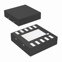
LMV712LD/NOPB National Semiconductor, LMV712LD/NOPB Datasheet - Page 11

LMV712LD/NOPB
Manufacturer Part Number
LMV712LD/NOPB
Description
IC OP AMP DUAL RR I/O W/SD 10LLP
Manufacturer
National Semiconductor
Datasheet
1.LMV712LDNOPB.pdf
(16 pages)
Specifications of LMV712LD/NOPB
Amplifier Type
General Purpose
Number Of Circuits
2
Output Type
Rail-to-Rail
Slew Rate
5 V/µs
Gain Bandwidth Product
5MHz
Current - Input Bias
5.5pA
Voltage - Input Offset
400µV
Current - Supply
1.17mA
Current - Output / Channel
50mA
Voltage - Supply, Single/dual (±)
2.7 V ~ 5.5 V
Operating Temperature
-40°C ~ 85°C
Mounting Type
Surface Mount
Package / Case
10-LLP
Lead Free Status / RoHS Status
Lead free / RoHS Compliant
-3db Bandwidth
-
Lead Free Status / Rohs Status
Details
Other names
LMV712LD
LMV712LDTR
LMV712LDTR
A glitch-free output waveform is highly desirable in many ap-
plications, one of which is power amplifier control loops. In
this application, the LMV712 is used to drive the power
amplifier's power control. If the LMV712 did not have a
smooth output ramp during turn on, it would directly cause the
power amplifier to produce a glitch at its output. This adverse-
ly affects the performance of the system.
To enable the amplifier, the shutdown pin must be pulled high.
It should not be left floating in the event that any leakage cur-
rent may inadvertently turn off the amplifier.
PRINTED CIRCUIT BOARD CONSIDERATION
To properly bypass the power supply, several locations on a
printed circuit board need to be considered. A 6.8µF or greater
tantalum capacitor should be placed at the point where the
power supply for the amplifier is introduced onto the board.
Another 0.1µF ceramic capacitor should be placed as close
as possible to the power supply pin of the amplifier. If the am-
plifier is operated in a single power supply, only the V
needs to be bypassed with a 0.1µF capacitor. If the amplifier
is operated in a dual power supply, both V
to be bypassed.
It is good practice to use a ground plane on a printed circuit
board to provide all components with a low inductive ground
connection.
Surface mount components in 0805 size or smaller are rec-
ommended in the LMV712 application circuits. Designers can
take advantage of the micro SMD, MSOP and LLP miniature
sizes to condense board layout in order to save space and
reduce stray capacitance.
CAPACITIVE LOAD TOLERANCE
The LMV712 can directly drive 200pF in unity-gain without
oscillation. The unity-gain follower is the most sensitive con-
figuration to capacitive loading. Direct capacitive loading re-
duces the phase margin of amplifiers. The combination of the
amplifier's output impedance and the capacitive load induces
phase lag. This results in either an under-damped pulse re-
sponse or oscillation. To drive a heavier capacitive load,
Figure 3
can be used.
FIGURE 3.
+
10137032
and V
−
pins need
+
pin
11
In
C
margin to the overall system. The desired performance de-
pends on the value of R
the more stable V
when the R
Figure
load resistor.
The circuit in
3
this circuit, R
ward techniques to connect V
counteract the loss of phase margin by feeding the high fre-
quency component of the output signal back to the amplifier's
inverting input, thereby preserving phase margin in the overall
feedback loop. Increased capacitive drive is possible by in-
creasing the value of C
response.
LATCHUP
CMOS devices tend to be susceptible to latchup due to their
internal parasitic SCR (silicon controlled rectifier) effects. The
input and output pins look similar to the gate of the SCR.
There is a minimum current required to trigger the SCR gate
lead. The LMV712 is designed to withstand 150mA surge
current on all the pins. Some resistive method should be used
to isolate any capacitance from supplying excess current to
the pins. In addition, like an SCR, there is a minimum holding
current for any latchup mode. Limiting current to the supply
pins will also inhibit latchup susceptibility.
L
because it provides DC accuracy as well as AC stability. In
Figure
form a pole to increase stability by adding more phase
3, the output voltage would be divided by R
3, the isolation resistor R
ISO
Figure 4
F
provides the DC accuracy by using feed-for-
gets bigger. If there were a load resistor in
OUT
will be. But the DC accuracy is degraded
is an improvement to the one in
F
ISO
. This in turn will slow down the pulse
FIGURE 4.
. The bigger the R
IN
to R
ISO
L
. C
and the load capacitor
F
and R
ISO
10137033
resistor value,
www.national.com
ISO
ISO
serve to
and the
Figure


