LMV712LD/NOPB National Semiconductor, LMV712LD/NOPB Datasheet - Page 4
LMV712LD/NOPB
Manufacturer Part Number
LMV712LD/NOPB
Description
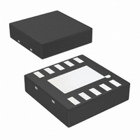
IC OP AMP DUAL RR I/O W/SD 10LLP
Manufacturer
National Semiconductor
Datasheet
1.LMV712LDNOPB.pdf
(16 pages)
Specifications of LMV712LD/NOPB
Amplifier Type
General Purpose
Number Of Circuits
2
Output Type
Rail-to-Rail
Slew Rate
5 V/µs
Gain Bandwidth Product
5MHz
Current - Input Bias
5.5pA
Voltage - Input Offset
400µV
Current - Supply
1.17mA
Current - Output / Channel
50mA
Voltage - Supply, Single/dual (±)
2.7 V ~ 5.5 V
Operating Temperature
-40°C ~ 85°C
Mounting Type
Surface Mount
Package / Case
10-LLP
Lead Free Status / RoHS Status
Lead free / RoHS Compliant
-3db Bandwidth
-
Lead Free Status / Rohs Status
Details
Other names
LMV712LD
LMV712LDTR
LMV712LDTR


www.national.com
V
V
I
A
V
GBWP
SR
φ
e
T
S
Symbol
n
ON
O
O
VOL
SD
m
Note 1: Absolute Maximum Ratings indicate limits beyond which damage to the device may occur. Operating Ratings indicate conditions for which the device is
intended to be functional, but specific performance is not guaranteed. For guaranteed specifications and the test conditions, see the Electrical Characteristics.
Note 2: Human Body Model, applicable std. MIL-STD-883, Method 3015.7. Machine Model, applicable std. JESD22-A115-A (ESD MM std. of JEDEC)
Field-Induced Charge-Device Model, applicable std. JESD22-C101-C (ESD FICDM std. of JEDEC).
Note 3: Shorting circuit output to either V
Note 4: The maximum power dissipation is a function of T
P
Note 5: Typical values represent the most likely parametric norm as determined at the time of characterization. Actual typical values may vary over time and will
also depend on the application and configuration. The typical values are not tested and are not guaranteed on shipped production material.
Note 6: All limits are guaranteed by testing or statistical analysis.
Note 7: Number specified is the slower of the positive and negative slew rates.
(SD)
D
= (T
J(MAX)
Output Swing
Output Voltage in Shutdown
Supply Current per Channel
Large Signal Voltage Gain
Shutdown Pin Voltage Range
Gain-Bandwidth Product
Slew Rate
Phase Margin
Input Referred Voltage Noise
Turn-On Time for Shutdown
Turn-On Time for Shutdown
– T
A
)/ θ
JA
. All numbers apply for packages soldered directly onto a PC Board.
Parameter
+
or V
−
will adversely affect reliability.
R
R
On Mode
Shutdown Mode
Sourcing
Sinking
Sourcing
Sinking
On Mode
Shutdown Mode
(Note
f = 1kHz
micro SMD
R
V
R
R
V
R
V
J(MAX)
L
L
V
L
O
L
L
O
L
O
= 10kΩ to 2.5V
= 600Ω to 2.5V
O
= 10kΩ
= 10kΩ
= 600Ω
= 600Ω
= 2.5V to 4.6V
= 2.5V to 4.6V
= 0.4V to 2.5V
, θ
= 0.4V to 2.5V
7)
JA
. The maximum allowable power dissipation at any ambient temperature is
Condition
4
(Note
4.5 to 5
0 to 0.8
4.92
4.90
4.82
4.80
Min
80
76
80
76
80
76
80
76
6
8
6)
(Note
3.5 to 5
0 to 1.5
4.98
0.01
4.85
0.05
1.17
0.12
Typ
130
130
110
107
1.6
10
60
20
5
5
5)
(Note
Max
0.12
0.15
0.23
0.30
200
1.7
1.9
1.5
2.0
4.6
4
6)
nV/
Units
MHz
V/µs
Deg
mV
mA
uA
dB
dB
dB
dB
μs
μs
V
V
V
V
V
V
Related parts for LMV712LD/NOPB
Image
Part Number
Description
Manufacturer
Datasheet
Request
R

Part Number:
Description:
IC,Operational Amplifier,DUAL,BICMOS,LLCC,10PIN,PLASTIC
Manufacturer:
National Semiconductor
Datasheet:
Part Number:
Description:
National Semiconductor [8-Bit D/A Converter]
Manufacturer:
National Semiconductor
Datasheet:
Part Number:
Description:
National Semiconductor [Media Coprocessor]
Manufacturer:
National Semiconductor
Datasheet:
Part Number:
Description:
Digitally Controlled Tone and Volume Circuit with Stereo Audio Power Amplifier, Microphone Preamp Stage and National 3D Sound
Manufacturer:
National Semiconductor
Datasheet:
Part Number:
Description:
Digitally Controlled Tone and Volume Circuit with Stereo Audio Power Amplifier, Microphone Preamp Stage and National 3D Sound
Manufacturer:
National Semiconductor
Datasheet:
Part Number:
Description:
AC97 Rev 2 Codec with Sample Rate Conversion and National 3D Sound
Manufacturer:
National Semiconductor
Part Number:
Description:
Manufacturer:
National Semiconductor
Datasheet:
Part Number:
Description:
Manufacturer:
National Semiconductor
Datasheet:
Part Number:
Description:
General Purpose, Low Voltage, Low Power, Rail-to-Rail Output Operational Amplifiers
Manufacturer:
National Semiconductor
Datasheet:
Part Number:
Description:
8-bit 20 MSPS flash A/D converter.
Manufacturer:
National Semiconductor
Datasheet:
Part Number:
Description:
Low Noise Quad Operational Amplifier
Manufacturer:
National Semiconductor
Datasheet:
Part Number:
Description:
Quad Differential Line Receivers
Manufacturer:
National Semiconductor
Datasheet:
Part Number:
Description:
Quad High Speed Trapezoidal? Bus Transceiver
Manufacturer:
National Semiconductor
Datasheet:
Part Number:
Description:
Dual Line Receiver
Manufacturer:
National Semiconductor
Datasheet: