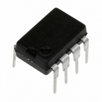
LF353N/NOPB National Semiconductor, LF353N/NOPB Datasheet - Page 2

LF353N/NOPB
Manufacturer Part Number
LF353N/NOPB
Description
IC OP AMP WB DUAL JFET IN 8-DIP
Manufacturer
National Semiconductor
Series
BI-FET II™r
Specifications of LF353N/NOPB
Amplifier Type
J-FET
Number Of Circuits
2
Slew Rate
13 V/µs
Gain Bandwidth Product
4MHz
Current - Input Bias
50pA
Voltage - Input Offset
5000µV
Current - Supply
3.6mA
Voltage - Supply, Single/dual (±)
10 V ~ 36 V, ±5 V ~ 18 V
Operating Temperature
0°C ~ 70°C
Mounting Type
Through Hole
Package / Case
8-DIP (0.300", 7.62mm)
Bandwidth
4 MHz
Channel Separation
-120
Common Mode Rejection Ratio
100
Current, Input Bias
50 pA
Current, Input Offset
25 pA
Current, Output
20 mA
Current, Supply
3.6 mA
Harmonic Distortion
0.02 %
Number Of Amplifiers
Dual
Package Type
MDIP-8
Resistance, Input
10^12 Ohms
Temperature, Operating, Range
0 to +70 °C
Voltage, Gain
100 V/mV
Voltage, Input
10 to 36 V
Voltage, Noise
16 nV/sqrt Hz
Voltage, Offset
5 mV
Voltage, Output, High
13.5 V
Voltage, Output, Low
-13.5 V
Voltage, Supply
±15 V
Dc
N/A
Lead Free Status / RoHS Status
Lead free / RoHS Compliant
Output Type
-
Current - Output / Channel
-
-3db Bandwidth
-
Lead Free Status / Rohs Status
RoHS Compliant part
Electrostatic Device
Other names
*LF353N
LF353
LF353NNS
LF353
LF353NNS
V
∆V
I
I
R
A
V
V
CMRR
PSRR
I
SR
GBW
e
i
n
OS
B
S
n
OS
VOL
O
CM
IN
Absolute Maximum Ratings
If Military/Aerospace specified devices are required,
please contact the National Semiconductor Sales Office/
Distributors for availability and specifications.
DC Electrical Characteristics
(Note 5)
AC Electrical Characteristics
(Note 5)
Symbol
Symbol
Supply Voltage
Power Dissipation
Operating Temperature Range
T
Differential Input Voltage
Input Voltage Range (Note 3)
Output Short Circuit Duration
Storage Temperature Range
Lead Temp. (Soldering, 10 sec.)
Soldering Information
OS
j
(MAX)
Dual-In-Line Package
/∆T
Soldering (10 sec.)
Amplifier to Amplifier Coupling
Slew Rate
Gain Bandwidth Product
Equivalent Input Noise Voltage
Equivalent Input Noise Current
Input Offset Voltage
Average TC of Input Offset Voltage
Input Offset Current
Input Bias Current
Input Resistance
Large Signal Voltage Gain
Output Voltage Swing
Input Common-Mode Voltage
Range
Common-Mode Rejection Ratio
Supply Voltage Rejection Ratio
Supply Current
Parameter
Parameter
−65˚C to +150˚C
0˚C to +70˚C
(Note 1)
Continuous
(Note 2)
150˚C
260˚C
260˚C
±
±
±
T
(Input Referred)
V
V
T
f=1000 Hz
T
18V
30V
15V
A
A
j
S
S
=25˚C, f=1000 Hz
=25˚C, f=1 Hz−20 kHz
=25˚C, R
=
=
R
Over Temperature
R
T
T
T
T
T
V
V
Over Temperature
V
V
R
(Note 7)
±
±
j
j
j
j
j
S
S
S
O
S
S
S
=25˚C, (Notes 5, 6)
≤70˚C
=25˚C, (Notes 5, 6)
≤70˚C
=25˚C
=
=
=
15V, T
15V, T
=10kΩ, T
=10 kΩ
=
≤ 10kΩ
±
±
±
±
15V, T
15V, R
15V
10V, R
Conditions
2
Conditions
S
A
A
=100Ω,
=25˚C
=25˚C
Note 1: Absolute Maximum Ratings indicate limits beyond which damage to
the device may occur. Operating ratings indicate conditions for which the
device is functional, but do not guarantee specific performance limits. Elec-
trical Characteristics state DC and AC electrical specifications under particu-
lar test conditions which guarantee specific performance limits. This assumes
that the device is within the Operating Ratings. Specifications are not guar-
anteed for parameters where no limit is given, however, the typical value is a
good indication of device performance.
See AN-450 “Surface Mounting Methods and Their Effect
on Product Reliability” for other methods of soldering
surface mount devices.
ESD Tolerance (Note 8)
θ
A
A
L
JA
L
=25˚C
=25˚C
=10kΩ
=2 kΩ
Small Outline Package
M Package
Vapor Phase (60 sec.)
Infrared (15 sec.)
Min
8.0
2.7
MIn
±
±
25
15
70
70
12
11
LF353
−120
LF353
0.01
±
Typ
10
13
16
Typ
+15
−12
100
100
100
4
3.6
13.5
10
25
50
5
12
Max
Max
100
200
6.5
10
13
4
8
1000V
215˚C
220˚C
Units
µV/˚C
Units
V/mV
V/mV
V/µs
MHz
TBD
mV
mV
mA
dB
pA
nA
pA
nA
dB
dB
Ω
V
V
V


