LF353N/NOPB National Semiconductor, LF353N/NOPB Datasheet - Page 3
LF353N/NOPB
Manufacturer Part Number
LF353N/NOPB
Description
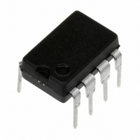
IC OP AMP WB DUAL JFET IN 8-DIP
Manufacturer
National Semiconductor
Series
BI-FET II™r
Specifications of LF353N/NOPB
Amplifier Type
J-FET
Number Of Circuits
2
Slew Rate
13 V/µs
Gain Bandwidth Product
4MHz
Current - Input Bias
50pA
Voltage - Input Offset
5000µV
Current - Supply
3.6mA
Voltage - Supply, Single/dual (±)
10 V ~ 36 V, ±5 V ~ 18 V
Operating Temperature
0°C ~ 70°C
Mounting Type
Through Hole
Package / Case
8-DIP (0.300", 7.62mm)
Bandwidth
4 MHz
Channel Separation
-120
Common Mode Rejection Ratio
100
Current, Input Bias
50 pA
Current, Input Offset
25 pA
Current, Output
20 mA
Current, Supply
3.6 mA
Harmonic Distortion
0.02 %
Number Of Amplifiers
Dual
Package Type
MDIP-8
Resistance, Input
10^12 Ohms
Temperature, Operating, Range
0 to +70 °C
Voltage, Gain
100 V/mV
Voltage, Input
10 to 36 V
Voltage, Noise
16 nV/sqrt Hz
Voltage, Offset
5 mV
Voltage, Output, High
13.5 V
Voltage, Output, Low
-13.5 V
Voltage, Supply
±15 V
Dc
N/A
Lead Free Status / RoHS Status
Lead free / RoHS Compliant
Output Type
-
Current - Output / Channel
-
-3db Bandwidth
-
Lead Free Status / Rohs Status
RoHS Compliant part
Electrostatic Device
Other names
*LF353N
LF353
LF353NNS
LF353
LF353NNS


THD
AC Electrical Characteristics
(Note 5)
Note 2: For operating at elevated temperatures, the device must be derated based on a thermal resistance of 115˚C/W typ junction to ambient for the N package,
and 158˚C/W typ junction to ambient for the H package.
Note 3: Unless otherwise specified the absolute maximum negative input voltage is equal to the negative power supply voltage.
Note 4: The power dissipation limit, however, cannot be exceeded.
Note 5: These specifications apply for V
Note 6: The input bias currents are junction leakage currents which approximately double for every 10˚C increase in the junction temperature, T
production test time, the input bias currents measured are correlated to junction temperature. In normal operation the junction temperature rises above the ambient
temperature as a result of internal power dissipation, P
recommended if input bias current is to be kept to a minimum.
Note 7: Supply voltage rejection ratio is measured for both supply magnitudes increasing or decreasing simultaneously in accordance with common practice. V
=
Note 8: Human body model, 1.5 kΩ in series with 100 pF.
Typical Performance Characteristics
Symbol
±
6V to
±
15V.
Total Harmonic Distortion
Input Bias Current
Supply Current
Parameter
S
=
±
15V and 0˚C≤T
D
. T
A
00564920
00564918
≤+70˚C. V
j
=T
(Continued)
A
+θ
A
V
BW=20 Hz-20 kHz
jA
V
O
P
=+10, RL=10k,
=20Vp−p,
OS
D
, I
where θ
B
and I
Conditions
3
OS
jA
is the thermal resistance from junction to ambient. Use of a heat sink is
are measured at V
Positive Common-Mode Input Voltage Limit
CM
=0.
Input Bias Current
Min
LF353
<
Typ
0.02
Max
j
. Due to the limited
00564919
00564921
Units
%
S
Related parts for LF353N/NOPB
Image
Part Number
Description
Manufacturer
Datasheet
Request
R

Part Number:
Description:
IC, OP-AMP, 4MHZ, 13V/µs, DIP-8
Manufacturer:
National Semiconductor
Datasheet:
Part Number:
Description:
National Semiconductor [8-Bit D/A Converter]
Manufacturer:
National Semiconductor
Datasheet:
Part Number:
Description:
National Semiconductor [Media Coprocessor]
Manufacturer:
National Semiconductor
Datasheet:
Part Number:
Description:
Digitally Controlled Tone and Volume Circuit with Stereo Audio Power Amplifier, Microphone Preamp Stage and National 3D Sound
Manufacturer:
National Semiconductor
Datasheet:
Part Number:
Description:
Digitally Controlled Tone and Volume Circuit with Stereo Audio Power Amplifier, Microphone Preamp Stage and National 3D Sound
Manufacturer:
National Semiconductor
Datasheet:
Part Number:
Description:
AC97 Rev 2 Codec with Sample Rate Conversion and National 3D Sound
Manufacturer:
National Semiconductor
Part Number:
Description:
Manufacturer:
National Semiconductor
Datasheet:
Part Number:
Description:
Manufacturer:
National Semiconductor
Datasheet:
Part Number:
Description:
General Purpose, Low Voltage, Low Power, Rail-to-Rail Output Operational Amplifiers
Manufacturer:
National Semiconductor
Datasheet:
Part Number:
Description:
8-bit 20 MSPS flash A/D converter.
Manufacturer:
National Semiconductor
Datasheet:
Part Number:
Description:
Low Noise Quad Operational Amplifier
Manufacturer:
National Semiconductor
Datasheet:
Part Number:
Description:
Quad Differential Line Receivers
Manufacturer:
National Semiconductor
Datasheet:
Part Number:
Description:
Quad High Speed Trapezoidal? Bus Transceiver
Manufacturer:
National Semiconductor
Datasheet:
Part Number:
Description:
Dual Line Receiver
Manufacturer:
National Semiconductor
Datasheet: