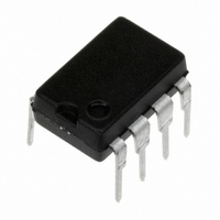
LF398N/NOPB National Semiconductor, LF398N/NOPB Datasheet - Page 3

LF398N/NOPB
Manufacturer Part Number
LF398N/NOPB
Description
IC AMP MONO SAMPLE & HOLD 8-DIP
Manufacturer
National Semiconductor
Specifications of LF398N/NOPB
Amplifier Type
Sample and Hold
Number Of Circuits
1
Current - Input Bias
10nA
Voltage - Input Offset
2000µV
Current - Supply
4.5mA
Voltage - Supply, Single/dual (±)
±5 V ~ 18 V
Operating Temperature
0°C ~ 70°C
Mounting Type
Through Hole
Package / Case
8-DIP (0.300", 7.62mm)
Current, Input Bias
10 nA
Current, Supply
4.5 mA
Impedance, Thermal
115 °C/W
Package Type
MDIP-8
Power Dissipation
500 mW
Temperature, Operating, Range
0 to +70 °C
Voltage, Input
±18 V
Voltage, Input Offset
2 mV
Voltage, Supply
±5 to ±18 V
Acquisition Time
4 us
Maximum Operating Temperature
+ 70 C
Minimum Operating Temperature
0 C
Supply Voltage (max)
18 V
Supply Voltage (min)
5 V
Lead Free Status / RoHS Status
Lead free / RoHS Compliant
Output Type
-
Current - Output / Channel
-
-3db Bandwidth
-
Slew Rate
-
Gain Bandwidth Product
-
Lead Free Status / Rohs Status
RoHS Compliant part
Electrostatic Device
Other names
*LF398N
*LF398N/NOPB
LF398
LF398N
LF398N/NOPB/NOPB
*LF398N/NOPB
LF398
LF398N
LF398N/NOPB/NOPB
Available stocks
Company
Part Number
Manufacturer
Quantity
Price
© 2000 National Semiconductor Corporation
LF198/LF298/LF398, LF198A/LF398A
Monolithic Sample-and-Hold Circuits
General Description
The LF198/LF298/LF398 are monolithic sample-and-hold
circuits which utilize BI-FET technology to obtain ultra-high
dc accuracy with fast acquisition of signal and low droop
rate. Operating as a unity gain follower, dc gain accuracy is
0.002% typical and acquisition time is as low as 6 µs to
0.01%. A bipolar input stage is used to achieve low offset
voltage and wide bandwidth. Input offset adjust is accom-
plished with a single pin, and does not degrade input offset
drift. The wide bandwidth allows the LF198 to be included in-
side the feedback loop of 1 MHz op amps without having sta-
bility problems. Input impedance of 10
source impedances to be used without degrading accuracy.
P-channel junction FET’s are combined with bipolar devices
in the output amplifier to give droop rates as low as 5 mV/min
with a 1 µF hold capacitor. The JFET’s have much lower
noise than MOS devices used in previous designs and do
not exhibit high temperature instabilities. The overall design
guarantees no feed-through from input to output in the hold
mode, even for input signals equal to the supply voltages.
Typical Connection and Performance Curve
Functional Diagram
DS005692
10
DS005692-32
allows high
Features
n Operates from
n Less than 10 µs acquisition time
n TTL, PMOS, CMOS compatible logic input
n 0.5 mV typical hold step at C
n Low input offset
n 0.002% gain accuracy
n Low output noise in hold mode
n Input characteristics do not change during hold mode
n High supply rejection ratio in sample or hold
n Wide bandwidth
n Space qualified, JM38510
Logic inputs on the LF198 are fully differential with low input
current, allowing direct connection to TTL, PMOS, and
CMOS. Differential threshold is 1.4V. The LF198 will operate
from
An “A” version is available with tightened electrical
specifications.
±
5V to
±
18V supplies.
±
5V to
Acquisition Time
DS005692-1
±
18V supplies
h
= 0.01 µF
DS005692-16


