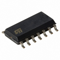
TS514IDT STMicroelectronics, TS514IDT Datasheet

TS514IDT
Specifications of TS514IDT
TS514IDT
Available stocks
Related parts for TS514IDT
TS514IDT Summary of contents
Page 1
Features Low input offset voltage: 500 μV max. ■ ■ Low power consumption. ■ Short circuit protection. ■ Low distortion, low noise. ■ High gain-bandwidth product. ■ High channel separation. ■ ESD protection 2 kV. ■ Macromodel included in this ...
Page 2
Absolute maximum ratings and operating conditions 1 Absolute maximum ratings and operating conditions Table 1. Absolute maximum ratings Symbol V Supply voltage CC V Input voltage i (1) Differential input voltage Storage temperature range stg Thermal resistance ...
Page 3
TS514 2 Schematic diagram Figure 1. Typical schematic diagram (1/4 TS514) Schematic diagram 3/16 ...
Page 4
Electrical characteristics 3 Electrical characteristics Table Symbol Supply current (per operator ≤ min Input bias current I – at 25° – min R Input resistance kHz ...
Page 5
TS514 Table Symbol Supply voltage rejection ratio, dV SVR V /V Channel separation kHz ± 25° C (unless otherwise specified) (continued) amb Parameter = ...
Page 6
Electrical characteristics Figure 2. Vio distribution at V T=25° distribution ° -400 -200 0 Input offset voltage (µV) Figure 4. Input offset voltage vs. supply voltage ...
Page 7
TS514 Figure 8. Supply current (per operator) vs. supply voltage at V 0.6 0.6 0.5 T=125°C T=25°C 0.4 0.4 0.3 0.2 0 icm 0 Supply voltage (V) ...
Page 8
Electrical characteristics Figure 14. Output current vs. output voltage T=-40°C 30 T=25° T=125° T=125°C -10 Sink -20 - -1V id ...
Page 9
TS514 Figure 20. Frequency response for different capacitive load and T=25° C icm 20 20 Gain with C =600 Gain with C =100 pF L -10 Gain with C -20 ...
Page 10
Electrical characteristics Figure 26. Phase margin vs. output current = and T=25° icm 70 Recommended area =100 =330 ...
Page 11
TS514 4 Package information In order to meet environmental requirements, ST offers these devices in ECOPACK packages. These packages have a Lead-free second level interconnect. The category of second level interconnect is marked on the package and on the inner ...
Page 12
Package information 4.1 DIP14 package information Figure 28. DIP14 package mechanical drawing Table 4. DIP14 package mechanical data Ref Note: D and E1 dimensions do not ...
Page 13
TS514 4.2 SO-14 package information Figure 29. SO-14 package mechanical drawing Table 5. SO-14 package mechanical data Ref ddd Note: D and F dimensions do not include mold ...
Page 14
... Ordering information 5 Ordering information Table 6. Order codes Order code TS514IN TS514AIN TS514ID TS514IDT TS514AID TS514AIDT (1) TS514IYD (1) TS514IYDT (1) TS514AIYD (1) TS514AIYDT 1. Qualification and characterization according to AEC Q100 and Q003 or equivalent, advanced screening according to AEC Q001 & Q 002 or equivalent are ongoing. 14/16 Temperature Package ...
Page 15
TS514 6 Revision history Table 7. Document revision history Date 09-Mar-2001 23-Jun-2005 30-Sep-2005 24-Oct-2008 Revision 1 Initial release. Automotive grade part references inserted in the datasheet 2 (see Chapter 5: Ordering information on page The following changes were made in ...
Page 16
... Information in this document is provided solely in connection with ST products. STMicroelectronics NV and its subsidiaries (“ST”) reserve the right to make changes, corrections, modifications or improvements, to this document, and the products and services described herein at any time, without notice. All ST products are sold pursuant to ST’s terms and conditions of sale. ...


