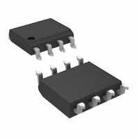
LMC6061AIM/NOPB National Semiconductor, LMC6061AIM/NOPB Datasheet

LMC6061AIM/NOPB
Specifications of LMC6061AIM/NOPB
*LMC6061AIM/NOPB
LMC6061AIM
Available stocks
Related parts for LMC6061AIM/NOPB
LMC6061AIM/NOPB Summary of contents
Page 1
... Low offset voltage: 100 µV Connection Diagram 8-Pin DIP/SO Top View © 2001 National Semiconductor Corporation n Ultra low supply current: 20 µA n Operates from 4.5V to 15V single supply n Ultra low input bias current Output swing within supply rail, 100k load n Input common-mode range includes V ...
Page 2
... Absolute Maximum Ratings If Military/Aerospace specified devices are required, please contact the National Semiconductor Sales Office/ Distributors for availability and specifications. Differential Input Voltage Voltage at Input/Output Pin + − Supply Voltage (V − Output Short Circuit to V − Output Short Circuit to V Lead Temperature (Soldering, 10 sec ...
Page 3
DC Electrical Characteristics Unless otherwise specified, all limits guaranteed for 1.5V 2.5V and Symbol Parameter + V Output Swing ...
Page 4
AC Electrical Characteristics Note 1: Absolute Maximum Ratings indicate limits beyond which damage to the device may occur. Operating Ratings indicate conditions for which the device is intended to be functional, but do not guarantee specific performance limits. For guaranteed ...
Page 5
Typical Performance Characteristics Distribution of LMC6061 Input Offset Voltage (T = +25˚C) A Distribution of LMC6061 Input Offset Voltage (T = +125˚C) A Supply Current vs Supply Voltage ± 7.5V 25˚C, Unless otherwise specified S A ...
Page 6
Typical Performance Characteristics specified (Continued) Common Mode Rejection Ratio vs Frequency Input Voltage Noise vs Frequency Output Characteristics Sinking Current www.national.com ± 7.5V 25˚C, Unless otherwise S A Power Supply Rejection 01142221 Output Characteristics 01142223 Gain ...
Page 7
Typical Performance Characteristics specified (Continued) Gain and Phase Response vs Capacitive Load with Open Loop Frequency Response Inverting Large Signal Pulse Response ± 7.5V 25˚C, Unless otherwise S A Response vs ...
Page 8
Typical Performance Characteristics specified (Continued) Non-Inverting Large Signal Pulse Response Stability vs Capacitive Load www.national.com ± 7.5V 25˚C, Unless otherwise S A Stability vs Capacitive 01142233 01142235 8 Load ...
Page 9
Applications Hints AMPLIFIER TOPOLOGY The LMC6061 incorporates a novel op-amp design topology that enables it to maintain rail-to-rail output swing even when driving a large load. Instead of relying on a push-pull unity gain output buffer stage, the output stage ...
Page 10
Applications Hints (Continued) PRINTED-CIRCUIT-BOARD LAYOUT FOR HIGH-IMPEDANCE WORK It is generally recognized that any circuit which must operate with less than 1000 pA of leakage current requires special layout of the PC board. When one wishes to take advantage of ...
Page 11
Applications Hints (Continued) Inverting Amplifier Non-Inverting Amplifier Follower FIGURE 5. Typical Connections of Guard Rings The designer should be aware that when it is inappropriate to lay out a PC board for the sake of just a few circuits, there ...
Page 12
Typical Single-Supply Applications + ( and then 100 for circuit shown (R = 9.822k ...
Page 13
Typical Single-Supply Applications + ( (Continued) DC Ordering Information Package 8-Pin Molded DIP 8-Pin Small Outline 8-Pin LMC6061AMJ/883 Ceramic DIP 01142213 FIGURE Square Wave Oscillator Temperature Range Military Industrial −55˚C to +125˚C −40˚C ...
Page 14
Physical Dimensions unless otherwise noted www.national.com inches (millimeters) 8-Pin Ceramic Dual-In-Line Package Order Number LMC6061AMJ/883 NS Package Number J08A 14 ...
Page 15
Physical Dimensions inches (millimeters) unless otherwise noted (Continued) Order Number LMC6061AIM, LMC6061AIMX, LMC6061IM or LMC6061IMX 8-Pin Small Outline Package NS Package Number M08A 8-Pin Molded Dual-In-Line Package Order Number LMC6061AIN or LMC6061IN NS Package Number N08E 15 www.national.com ...
Page 16
... NATIONAL’S PRODUCTS ARE NOT AUTHORIZED FOR USE AS CRITICAL COMPONENTS IN LIFE SUPPORT DEVICES OR SYSTEMS WITHOUT THE EXPRESS WRITTEN APPROVAL OF THE PRESIDENT AND GENERAL COUNSEL OF NATIONAL SEMICONDUCTOR CORPORATION. As used herein: 1. Life support devices or systems are devices or systems which, (a) are intended for surgical implant ...


