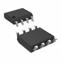
LMC6061AIM/NOPB National Semiconductor, LMC6061AIM/NOPB Datasheet - Page 9

LMC6061AIM/NOPB
Manufacturer Part Number
LMC6061AIM/NOPB
Description
IC OP AMP CMOS SINGL MICRO 8SOIC
Manufacturer
National Semiconductor
Specifications of LMC6061AIM/NOPB
Amplifier Type
General Purpose
Number Of Circuits
1
Output Type
Rail-to-Rail
Slew Rate
0.35 V/µs
Gain Bandwidth Product
100kHz
Current - Input Bias
0.01pA
Voltage - Input Offset
100µV
Current - Supply
24µA
Current - Output / Channel
26mA
Voltage - Supply, Single/dual (±)
4.5 V ~ 15.5 V, ±2.25 V ~ 7.75 V
Operating Temperature
-40°C ~ 85°C
Mounting Type
Surface Mount
Package / Case
8-SOIC (3.9mm Width)
Bandwidth
100 kHz
Common Mode Rejection Ratio
85
Current, Input Bias
0.01 pA
Current, Input Offset
0.005 pA
Current, Output
22 mA
Current, Supply
20 μA
Harmonic Distortion
0.01 %
Impedance, Thermal
193 °C/W
Number Of Amplifiers
Single
Package Type
SO-8
Resistance, Input
10 Teraohms
Temperature, Operating, Range
-40 to +85 °C
Voltage, Gain
4000 V/mV
Voltage, Input
4.5 to 15.5 V
Voltage, Noise
83 nV/sqrt Hz
Voltage, Offset
100 μV
Voltage, Output, High
4.995 V
Voltage, Output, Low
0.005 V
Voltage, Supply
5 V
Number Of Channels
1
Voltage Gain Db
132.04 dB
Common Mode Rejection Ratio (min)
75 dB
Input Voltage Range (max)
15.5 V
Input Voltage Range (min)
4.5 V
Input Offset Voltage
0.35 mV at 5 V
Operating Supply Voltage
5 V, 9 V, 12 V, 15 V
Supply Current
0.024 mA at 5 V
Maximum Operating Temperature
+ 85 C
Mounting Style
Through Hole
Minimum Operating Temperature
- 40 C
Lead Free Status / RoHS Status
Lead free / RoHS Compliant
-3db Bandwidth
-
Lead Free Status / Rohs Status
RoHS Compliant part
Electrostatic Device
Other names
*LMC6061AIM
*LMC6061AIM/NOPB
LMC6061AIM
*LMC6061AIM/NOPB
LMC6061AIM
Available stocks
Company
Part Number
Manufacturer
Quantity
Price
Part Number:
LMC6061AIM/NOPB
Manufacturer:
TI/德州仪器
Quantity:
20 000
Applications Hints
AMPLIFIER TOPOLOGY
The LMC6061 incorporates a novel op-amp design topology
that enables it to maintain rail-to-rail output swing even when
driving a large load. Instead of relying on a push-pull unity
gain output buffer stage, the output stage is taken directly
from the internal integrator, which provides both low output
impedance and large gain. Special feed-forward compensa-
tion design techniques are incorporated to maintain stability
over a wider range of operating conditions than traditional
micropower op-amps. These features make the LMC6061
both easier to design with, and provide higher speed than
products typically found in this ultra-low power class.
COMPENSATING FOR INPUT CAPACITANCE
It is quite common to use large values of feedback resis-
tance for amplifiers with ultra-low input current, like the
LMC6061.
Although the LMC6061 is highly stable over a wide range of
operating conditions, certain precautions must be met to
achieve the desired pulse response when a large feedback
resistor is used. Large feedback resistors and even small
values of input capacitance, due to transducers, photo-
diodes, and circuit board parasitics, reduce phase margins.
When high input impedances are demanded, guarding of the
LMC6061 is suggested. Guarding input lines will not only
reduce leakage, but lowers stray input capacitance as well.
(See Printed-Circuit-Board Layout for High Impedance
Work ).
The effect of input capacitance can be compensated for by
adding a capacitor. Place a capacitor, C
back resistor (as in Figure 1 ) such that:
Since it is often difficult to know the exact value of C
be experimentally adjusted so that the desired pulse re-
sponse is achieved. Refer to the LMC660 and the LMC662
for a more detailed discussion on compensating for input
capacitance.
CAPACITIVE LOAD TOLERANCE
All rail-to-rail output swing operational amplifiers have volt-
age gain in the output stage. A compensation capacitor is
normally included in this integrator stage. The frequency
FIGURE 1. Canceling the Effect of Input Capacitance
R
1
C
IN
or
R
2
C
f
f
, around the feed-
01142205
IN
, C
f
can
9
location of the dominate pole is affected by the resistive load
on the amplifier. Capacitive load driving capability can be
optimized by using an appropriate resistive load in parallel
with the capacitive load (see typical curves).
Direct capacitive loading will reduce the phase margin of
many op-amps. A pole in the feedback loop is created by the
combination of the op-amp’s output impedance and the ca-
pacitive load. This pole induces phase lag at the unity-gain
crossover frequency of the amplifier resulting in either an
oscillatory or underdamped pulse response. With a few ex-
ternal components, op amps can easily indirectly drive ca-
pacitive loads, as shown in Figure 2 .
In the circuit of Figure 2 , R1 and C1 serve to counteract the
loss of phase margin by feeding the high frequency compo-
nent of the output signal back to the amplifier’s inverting
input, thereby preserving phase margin in the overall feed-
back loop.
Capacitive load driving capability is enhanced by using a pull
up resistor to V
ducting 10 µA or more will significantly improve capacitive
load responses. The value of the pull up resistor must be
determined based on the current sinking capability of the
amplifier with respect to the desired output swing. Open loop
gain of the amplifier can also be affected by the pull up
resistor (see electrical characteristics).
FIGURE 2. LMC6061 Noninverting Gain of 10 Amplifier,
Compensated to Handle Capacitive Loads
Capacitive Loads with a Pull Up Resistor
FIGURE 3. Compensating for Large
+
Figure 3 . Typically a pull up resistor con-
01142214
www.national.com
01142204


