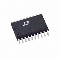
LT1795CSW#TR Linear Technology, LT1795CSW#TR Datasheet - Page 10

LT1795CSW#TR
Manufacturer Part Number
LT1795CSW#TR
Description
IC AMP CURR FEEDBACK DUAL 20SOIC
Manufacturer
Linear Technology
Datasheet
1.LT1795CSW.pdf
(12 pages)
Specifications of LT1795CSW#TR
Amplifier Type
Current Feedback
Number Of Circuits
2
Slew Rate
900 V/µs
-3db Bandwidth
65MHz
Current - Input Bias
10µA
Voltage - Input Offset
3000µV
Current - Supply
29mA
Current - Output / Channel
1A
Voltage - Supply, Single/dual (±)
±5 V ~ 15 V
Operating Temperature
0°C ~ 70°C
Mounting Type
Surface Mount
Package / Case
20-SOIC (7.5mm Width)
Lead Free Status / RoHS Status
Contains lead / RoHS non-compliant
Output Type
-
Gain Bandwidth Product
-
Lead Free Status / Rohs Status
Not Compliant
Available stocks
Company
Part Number
Manufacturer
Quantity
Price
APPLICATIONS
LT1795
PACKAGE DESCRIPTIO
10
Figure 9 shows the effect of the network on a 200pF load.
Without the optional compensation, there is a 6dB peak at
85MHz caused by the effect of the capacitance on the
output stage. Adding a 0.01 F bypass capacitor between
the output and the COMP pins connects the compensation
14
12
10
–2
–4
–6
8
6
4
2
0
1
V
C
S
L
= 15V
= 200pF
R
COMPENSATION
F
U
.030 .005
NOTE:
1. DIMENSIONS IN
2. DRAWING NOT TO SCALE
3. PIN 1 IDENT, NOTCH ON TOP AND CAVITIES ON THE BOTTOM OF PACKAGES ARE THE MANUFACTURING OPTIONS.
4. THESE DIMENSIONS DO NOT INCLUDE MOLD FLASH OR PROTRUSIONS.
= 1k
RAD MIN
(0.229 – 0.330)
(0.127)
.009 – .013
THE PART MAY BE SUPPLIED WITH OR WITHOUT ANY OF THE OPTIONS
MOLD FLASH OR PROTRUSIONS SHALL NOT EXCEED .006" (0.15mm)
.005
TYP
.420
MIN
FREQUENCY (MHz)
INFORMATION
Figure 9
U
RECOMMENDED SOLDER PAD LAYOUT
N
1
10
(MILLIMETERS)
(0.254 – 0.737)
2
INCHES
.010 – .029
NOTE 3
COMPENSATION
R
COMPENSATION
(7.391 – 7.595)
F
.291 – .299
= 3.4k
NOTE 4
W
R
3
(0.406 – 1.270)
F
.016 – .050
= 3.4k
NO
U
20-Lead Plastic Small Outline (Wide .300 Inch)
45
1795 F09
.050 BSC
100
N/2
(Reference LTC DWG # 05-08-1620)
U
.325 .005
.045 .005
0 – 8 TYP
NOTE 3
SW Package
(2.362 – 2.642)
.093 – .104
(1.270)
.050
BSC
and greatly reduces the peaking. A lower value feedback
resistor can now be used, resulting in a response which is
flat to 1dB to 45MHz. The network has the greatest effect
for C
Although the optional compensation works well with
capacitive loads, it simply reduces the bandwidth when it
is connected with resistive loads. For instance, with a 25
load, the bandwidth drops from 48MHz to 32MHz when
the compensation is connected. Hence, the compensation
was made optional. To disconnect the optional compensa-
tion, leave the COMP pin open.
DEMO BOARD
A demo board (DC261A) is available for evaluating the
performence of the LT1795. The board is configured as a
differential line driver/receiver suitable for xDSL applica-
tions. For details, consult your local sales representative.
20
N
1
(0.356 – 0.482)
.014 – .019
19
2
TYP
L
18
3
in the range of 0pF to 1000pF.
17
(12.598 – 13.005)
4
.496 – .512
16
NOTE 4
5
15
6
14
7
13
8
12
9
N/2
11
10
(0.940 – 1.143)
.037 – .045
(0.102 – 0.305)
(10.007 – 10.643)
.004 – .012
.394 – .419
S20 (WIDE) 0502
1795fa


